 ALLPCB


Introduction
Flexible printed circuit boards, known as flex PCBs, have become essential in modern electronics where space constraints and mechanical movement are common. Dynamic flexing applications, such as wearable devices, robotic arms, and foldable displays, require these boards to endure millions of bend cycles without failure. The key to reliability lies in optimizing flex PCB thickness for dynamic bending, which directly influences the achievable PCB bend radius. Engineers must balance thinner profiles for tighter bends against risks like copper cracking or delamination. This article delves into the engineering principles, standards-driven guidelines, and best practices to help select the right thickness. By understanding these factors, designers can enhance product longevity and performance in demanding environments.

Understanding Flex PCB Thickness and Its Role in Dynamic Applications
Flex PCB thickness refers to the total stack-up height, including copper foils, dielectric layers like polyimide, and adhesives. In dynamic flexing applications, this parameter determines the minimum PCB bend radius, as strain concentrates on the outer copper layers during flexion. Thinner constructions allow smaller bend radii, enabling compact designs, but they increase vulnerability to fatigue from repeated cycles. Industry standards classify flex applications as static for occasional bends or dynamic for continuous motion exceeding 1,000 cycles. Why does this matter for electric engineers? Poor thickness optimization leads to field failures, increased warranty costs, and redesign iterations, underscoring the need for precise calculations from the outset.
The relationship between thickness and bend radius follows a proportional model where radius equals a factor multiplied by thickness. Factors vary by layer count, copper ductility, and application type, ensuring outer fiber strain stays below material limits. For instance, rolled annealed copper offers better flex endurance than electrodeposited types due to its grain structure. Engineers evaluate total thickness early in design to predict performance under operational stresses like vibration or thermal cycling. This proactive approach aligns with factory production capabilities, minimizing yield losses during high-volume manufacturing.
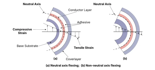
Technical Principles Governing Flex PCB Thickness and Bend Radius
The core principle behind flex PCB thickness for dynamic bending is managing mechanical strain on conductors. When a flex PCB bends, the neutral axis shifts slightly, placing tensile strain on the outer copper and compressive on the inner. To prevent cracking, the bend radius must exceed a minimum value based on thickness, typically expressed as a ratio. IPC-2223 provides detailed guidelines for these ratios, distinguishing between single-conductor, multilayer, and dynamic scenarios. Thinner dielectrics reduce overall stack height, lowering strain for a given radius, but require finer line widths to maintain impedance control.
Copper thickness significantly impacts durability, as thicker foils resist cracking longer but demand larger radii. Polyimide films, common at 12.5 to 50 microns, offer high flexibility, yet adhesive layers can introduce peel risks under cyclic loading. Finite element analysis simulates strain distribution, revealing hotspots at vias or terminations. Temperature exacerbates issues, as materials stiffen below glass transition points, tightening effective radii. Vibration in dynamic flexing applications amplifies these effects, necessitating margin in thickness selection.
Material properties like modulus of elasticity dictate bend behavior. Softer substrates enable tighter bends, but signal integrity suffers from higher insertion loss in high-frequency dynamic flexing applications. Adhesiveless laminates eliminate weak interfaces, supporting thinner stacks for aggressive radii. Conductor patterning, such as teardrops at bends, redistributes stress. These principles ensure the PCB bend radius remains achievable without exceeding yield strain, typically 10% elongation for flex copper.
Factors Influencing Optimal Flex PCB Thickness Selection
Several interrelated factors guide flex PCB thickness choices for dynamic bending. Layer count is primary: single-layer boards tolerate ratios around 100:1 for dynamic use, while multilayers escalate to 200:1 or higher. Copper weight, from 1/2 oz to 2 oz per ft2, trades off current capacity against flexibility. Dielectric thickness scales with copper to maintain balance, often 25 microns per side for fine-pitch designs. Environmental exposure, like humidity or chemicals, demands robust coverlays to protect thinned sections.
Manufacturing tolerances affect effective thickness, with etch back and plating adding variability. Factory processes like lamination pressure influence voiding, critical for thin stacks prone to microcracks. Signal requirements dictate minimum thickness for controlled impedance, especially in high-speed dynamic flexing applications. Mechanical reinforcements, such as stiffeners, allow hybrid thin-flex regions. Engineers iterate stack-ups using design rules to hit target PCB bend radius while meeting electrical specs.
Thermal management poses challenges, as thin flex dissipates heat poorly during dynamic motion. Coefficient of thermal expansion mismatches between copper and polyimide induce additional strain over cycles. Testing validates choices, revealing fatigue life correlations with thickness. Comprehensive consideration prevents over-design, which bloats costs, or under-design, which risks early failure.
Best Practices for Optimizing Flex PCB Thickness in Production
Start with application profiling to classify bend cycles and amplitude, informing thickness targets. Reference IPC-2223 ratios as baselines: for double-layer dynamic, aim for 150 times thickness minimum. Prototype thin stacks iteratively, measuring bend radius with mandrels. Incorporate generous fillets on traces and avoid right angles in flex zones to distribute stress evenly. Select ductile copper and thin polyimide for dynamic flexing applications, verifying supplier specs align with design.
During layout, zone the board with dedicated flex areas, tapering thickness where possible. Simulate dynamic loading with software to predict cycle life versus PCB bend radius. Factory qualification per IPC-6013 ensures performance, including flexural endurance tests. Collaborate early with manufacturers on DFM reviews, adjusting for process windows like coverlay alignment on thin profiles. Monitor plating uniformity, as inconsistencies amplify strain in bends.

Post-production, implement incoming inspections for thickness variation using micrometers or ultrasonics. Field data logging tracks real-world flex PCB thickness for dynamic bending performance, refining future designs. These practices yield robust boards, extending mean time between failures in critical applications.
Troubleshooting Common Issues in Dynamic Flex PCB Designs
Engineers often encounter cracking at bend edges due to insufficient radius relative to thickness. Diagnose by sectioning failed samples, revealing copper fatigue facets under microscopy. Remedy involves increasing dielectric thinness or switching to finer copper. Delamination signals adhesive weakness; opt for adhesiveless builds in high-cycle zones.
Vibration-induced opens trace to trace rollover; reinforce with patterned grounds. Impedance drift in thin stacks requires precise width control. Thermal cycling failures highlight CTE mismatches; validate with accelerated life tests. Systematic root cause analysis, tied to thickness metrics, resolves most issues efficiently.
Conclusion
Optimizing flex PCB thickness for dynamic bending demands a holistic approach integrating material science, standards, and testing. Key is adhering to PCB bend radius ratios from established guidelines, balancing thinness for compactness against durability. Practical implementation through simulation, prototyping, and qualification minimizes risks in dynamic flexing applications. Electric engineers benefit from factory-aligned designs that deliver reliable performance over product lifecycles. Prioritizing these elements ensures innovation without compromise.
FAQs
Q1: What is the typical PCB bend radius for dynamic flexing applications using a 0.1 mm thick single-layer flex PCB?
A1: Industry guidelines recommend a minimum ratio of 100:1 for single-layer dynamic use, yielding a 10 mm bend radius. This prevents excessive strain on copper, supporting millions of cycles. Verify with flexural testing to account for specific materials and environments. Thinner profiles enhance flexibility but require precise manufacturing.
Q2: How does flex PCB thickness for dynamic bending impact fatigue life?
A2: Thinner thicknesses enable smaller PCB bend radius but accelerate fatigue if ratios are violated, leading to cracking after fewer cycles. Standards suggest scaling radius proportionally to total stack height for endurance. Balance with copper ductility and dielectric properties. Testing under simulated conditions quantifies life improvements from optimized thickness.
Q3: What factors should engineers consider when selecting flex PCB thickness for dynamic bending?
A3: Layer count, copper type, and cycle frequency dictate minimum ratios per design standards. Signal integrity and thermal performance constrain thinning limits. Manufacturing tolerances and reinforcements influence feasibility. Comprehensive stack-up analysis ensures reliable dynamic flexing applications.
Q4: Can flex PCB thickness be varied within a single board for better PCB bend radius control?
A4: Yes, zoned designs with thinned flex areas and stiffened sections optimize performance. This hybrid approach accommodates tight bends where needed while maintaining rigidity elsewhere. Adhere to transition guidelines to avoid stress concentrations. Validation testing confirms integrity across variations.
References
IPC-2223C — Sectional Design Standard for Flexible Printed Boards. IPC.
IPC-6013E — Qualification and Performance Specification for Flexible Printed Boards. IPC.
IPC-TM-650 2.4.3 — Flexural Fatigue Test Method. IPC.


