 ALLPCB


Introduction
Flexible PCBs have revolutionized electronics by enabling compact, bendable designs in applications ranging from wearables to medical devices. Panelization, the process of arranging multiple individual flexible circuits on a larger production panel, is essential for optimizing PCB assembly and minimizing manufacturing costs. However, determining the optimal panel size introduces specific PCB challenges flexi, such as warpage and handling difficulties inherent to thin, pliable materials. Engineers must balance material utilization with structural integrity to ensure high yields during fabrication and assembly. Larger panels maximize throughput but amplify risks like dimensional instability, while smaller ones may increase per-unit expenses. This article delves into these challenges and provides practical techniques for achieving reliable flexible PCB panels.
Understanding Panelization for Flexible PCBs and Why Optimal Size Matters
Panelization groups multiple small flexi arrays onto a single panel to streamline processes like etching, lamination, and soldering. For flexible PCBs, standard rigid panel dimensions around 18 by 24 inches serve as a starting point, but adjustments are necessary due to material properties like polyimide's high flexibility and low rigidity. Optimal panel size directly impacts yield, as oversized panels lead to uneven stress distribution during thermal cycling. In optimizing PCB assembly, proper sizing ensures compatibility with pick-and-place machines and reflow ovens, reducing defects from misalignment. Industry relevance stems from cost savings; efficient panelization can boost material usage from typical levels to over 90 percent in well-designed layouts. Engineers prioritizing bendable component placement must consider how panel size affects tolerances for dynamic flex areas.
The economic stakes are high in high-volume production, where suboptimal sizing results in scrap rates climbing due to handling errors. Flexible PCBs demand panels that accommodate stiffeners or carriers without compromising bend radii. As per IPC-6013 guidelines, panel design must maintain performance specifications across varied sizes. Ignoring these factors leads to assembly bottlenecks, particularly in small flexi array configurations where edge effects dominate.
Key Technical Challenges in Flexible PCB Panel Sizing
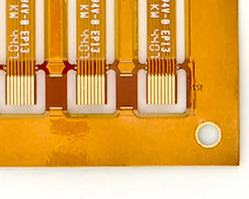
One primary challenge is warpage, caused by coefficient of thermal expansion mismatches between copper foils and base films during lamination and soldering. Thin flexible substrates, often under 0.25 mm, exhibit pronounced bowing when panelized in large formats, exceeding allowable limits and causing pick-and-place failures. Handling floppy panels risks tears or creases, especially in multi-layer stacks where interlayer adhesion varies. PCB challenges flexi intensify in humid environments, as moisture absorption alters dimensions unpredictably.
Dimensional stability poses another hurdle, with shrinkage during curing leading to fiducial misalignment in optimizing PCB assembly. Bendable component placement becomes problematic in oversized panels, as flex zones stretch unevenly under conveyor tension. Vibration during transport amplifies these issues, potentially delaminating coverlays. Standards like IPC-2223 emphasize minimum border widths to mitigate edge curling, yet large panels strain compliance.
Assembly-specific obstacles include thermal gradients across extended panels, resulting in uneven reflow and solder joint voids. Small flexi arrays on large panels suffer from unsupported peripheries, complicating stencil alignment. Thin materials also limit V-scoring depth, favoring tab routing that increases depaneling stress. These factors collectively demand a nuanced approach to size selection.
Engineering Principles Governing Panel Size Selection
Material science principles dictate that panel aspect ratios should stay below 2:1 to distribute mechanical stresses evenly. Polyimide's high glass transition temperature aids stability, but copper's rigidity creates bow-and-twist moments proportional to panel area. Finite element analysis reveals warpage scaling quadratically with size, guiding engineers to cap dimensions based on substrate thickness. Cooling rates post-lamination influence residual stresses, with slower profiles reducing curvature in flexible PCBs.
Handling dynamics require considering panel mass and gripper compatibility; overly large formats exceed vacuum chuck capacities. In bendable component placement, trace routing must account for strain concentrations at panel edges, per design standards. Thermal mass variations affect reflow profiles, where central circuits overheat relative to borders. Optimal sizing integrates these mechanisms for predictable behavior.
Practical Techniques and Best Practices for Optimal Panel Sizing
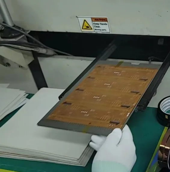
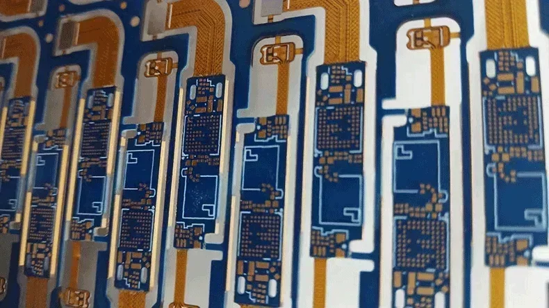
Start by evaluating equipment constraints: match panel dimensions to printer beds and oven zones, typically favoring 12 by 18 inches for flex to limit warpage below 0.75 percent. Incorporate 5 to 10 mm borders with tooling holes and fiducials spaced per IPC-6013 for precise registration. Use perforated tabs over full rails in small flexi arrays to ease depaneling without tearing flex tails.
For optimizing PCB assembly, employ rigid carriers taped to flex panels, providing mechanical support during stencil printing and placement. Symmetrical layouts minimize asymmetry-induced twist, with up to 20 circuits per panel yielding best utilization. Simulate warpage using thermal-mechanical models to iterate sizes pre-production. Stiffener placement near bend zones enhances bendable component placement stability.
Advanced techniques include zoned lamination, applying pressure gradients to counteract shrinkage. Partial etching of carrier frames allows peel-off post-assembly, preserving flex integrity. Material selection favors low-CTE adhesives to stabilize multi-layer panels. Regular bow-and-twist measurements during trials refine sizing iteratively.
In high-density small flexi array designs, nest irregular shapes with 1 mm gaps to maximize density while avoiding interference. Post-bake stabilization at controlled temperatures preconditions panels against reflow stresses. Collaborative DFM reviews with fabricators ensure size aligns with routing capabilities.
Troubleshooting Common Issues in Flex Panel Production
Engineers often encounter excessive warpage in initial runs; counter this by reducing panel count or adding symmetric dummy circuits. Misalignment during assembly signals inadequate fiducials; upgrade to 1 mm diameter, high-contrast pads. Handling damage appears as micro-cracks; mitigate with anti-static films and edge beveling.
Delamination in humid conditions traces to poor coverlay adhesion; verify per IPC-6013 and adjust cure cycles. For bendable component placement failures, reinforce pads with anchor vias. These targeted fixes restore yield without resizing.
Conclusion
Achieving optimal panel size for flexible PCBs requires addressing PCB challenges flexi through balanced design and process controls. Key techniques like carrier use, symmetrical layouts, and standards compliance ensure stability in optimizing PCB assembly. By prioritizing warpage mitigation and handling aids, engineers unlock efficient production of small flexi arrays with reliable bendable component placement. Implementing these strategies yields cost-effective, high-performance flexible PCBs ready for demanding applications.
FAQs
Q1: What are the main PCB challenges flexi when panelizing large flexible PCBs?
A1: Warpage from thermal stresses and handling difficulties due to thin substrates top the list. Large panels amplify CTE mismatches, leading to bow exceeding 0.75 percent and pick-and-place errors. Proper border design and carriers per IPC-6013 mitigate these, ensuring assembly compatibility. Optimal sizing under 18 by 24 inches balances yield and stability.
Q2: How does optimizing PCB assembly benefit from specific panel sizes for flexible PCBs?
A2: Tailored sizes match SMT equipment, reducing misalignment and reflow defects. Smaller panels minimize thermal gradients, improving solder joint quality in bendable areas. Carriers enable standard handling, boosting throughput for small flexi arrays. This approach cuts scrap and accelerates production cycles.
Q3: Why is bendable component placement tricky in small flexi array panels?
A3: Flex zones strain under depaneling forces, risking trace cracks near edges. Unsupported peripheries cause vibration-induced shifts during placement. Stiffeners and fiducials stabilize components, with tab routing preferred over scoring. Standards like IPC-2223 guide pad anchoring for durability.
Q4: What techniques achieve optimal panel size without sacrificing material efficiency?
A4: Symmetrical nesting maximizes circuit count within equipment limits. Dummy fills counter asymmetry, while simulation predicts warpage. Perforated frames allow high utilization above 85 percent. Iterative DFM ensures compliance with flex-specific tolerances.
References
IPC-6013 — Qualification and Performance Specification for Flexible Printed Boards. IPC
IPC-2223 — Sectional Design Standard for Flexible Printed Boards. IPC
J-STD-001 — Requirements for Soldered Electrical and Electronic Assemblies. IPC


