ALLPCB


Since the 2019 rollout of 5G, deployment has accelerated. RF front-end chips are among the biggest beneficiaries. According to Yole, the global RF front-end market is projected to reach $21.67 billion by 2026, up from $12.41 billion in 2019, a 74.6% increase over seven years.
What is the RF front end?
The RF front end is the functional module between the antenna and the transceiver in wireless communication systems. Because it sits at the front of the communication chain, it is called the RF front end and typically includes power amplifiers, filters/duplexers, switches, and low-noise amplifiers.
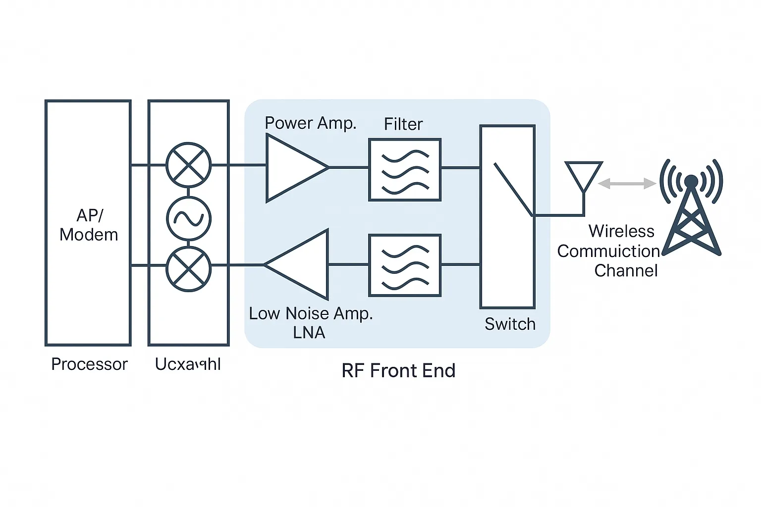
Figure: RF front-end composition and functions
Role of the power amplifier (PA)
The RF power amplifier, or PA, is a key component in the RF front end whose performance directly affects signal strength, stability, power consumption, and user experience. Core parameters include gain, bandwidth, efficiency, linearity, and maximum output power. Balancing these metrics is a significant design challenge.
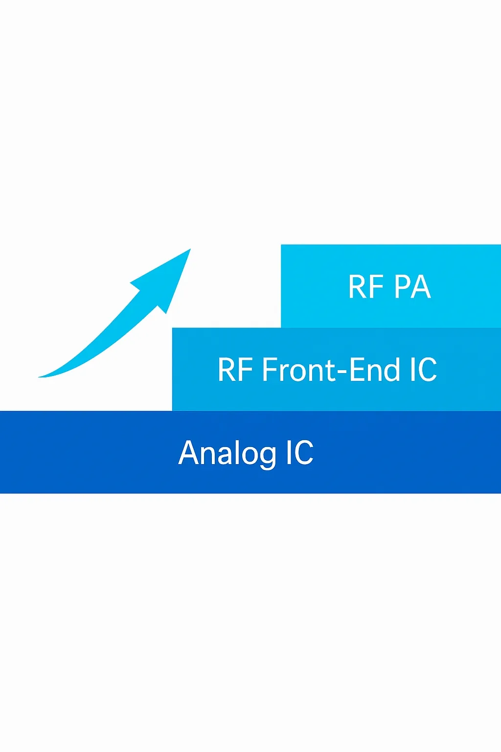
Figure: PA position within a chip design
With 5G, PA requirements have increased: higher operating frequency, higher output power, wider bandwidth, and higher integration for modular RF modules. Various PA architectures beyond simple single-ended PAs are now used in mobile applications, including push-pull, balance, and Doherty PAs. This article reviews these architectures, their principles, and their characteristics.
PA design principles
A PA is optimized for power output rather than just gain, unlike low-noise or driver amplifiers. To achieve high power, PAs typically forgo conjugate matching used for maximum power transmission and instead use load-line matching to enable maximum power output. Efficiency optimization is also a primary design consideration to control DC power consumption.
Load-line matching maximizes both voltage and current swing at the device, achieving maximum output power.
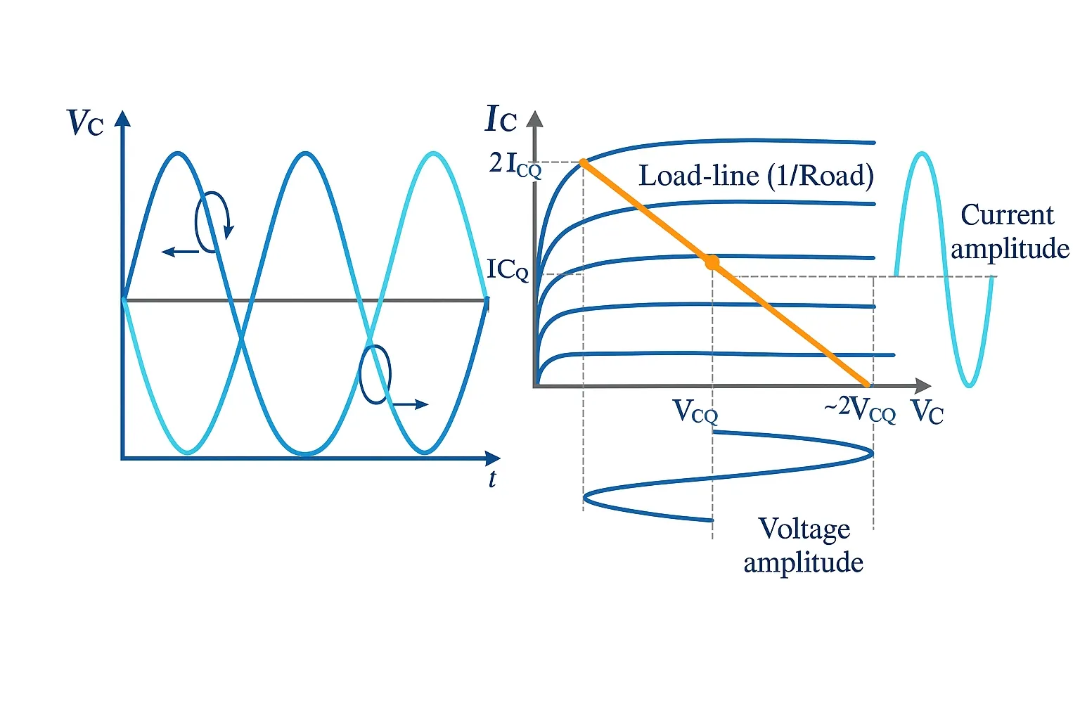
Figure: Load-line theory and voltage/current swing
In practice, a single PA device might not provide sufficient voltage or current swing to meet system requirements, so architecture-level techniques are used to improve efficiency or standing-wave behavior.
PA architecture overview
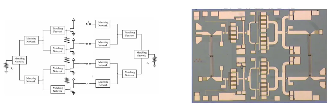
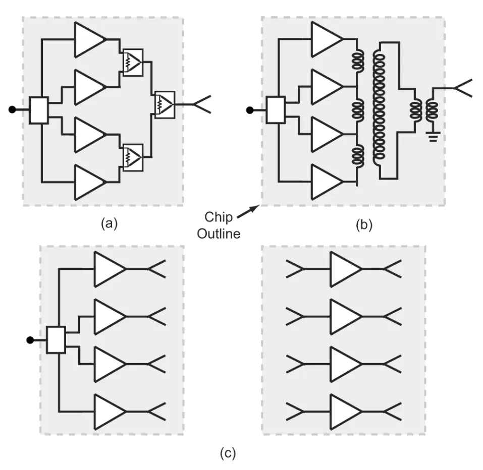
The core objective of any PA is power. PA architectures are centered on power combining. Power combining can be classified as simple power combining or special power combining.
Simple power combining aggregates multiple lower-power devices until the required power is achieved. Methods include current combining, voltage combining, and general power combining. Special power combining uses more advanced techniques to realize additional characteristics during combining, such as push-pull, balance, and Doherty architectures.
Simple power combining
Current combining
Current combining is the simplest approach: multiple smaller devices are connected in parallel so their currents sum. In layout, collectors, bases, and emitters of multiple transistors are connected. Because of its simplicity, current combining is widely used in PA designs.
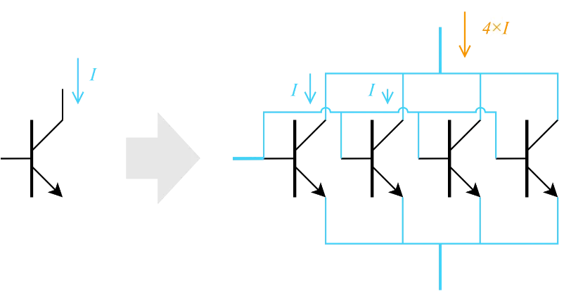
Figure: Current combining in power amplifiers
Typical GaAs PA layouts show power output stages formed by power arrays—multiple power cells connected to achieve the final output power.
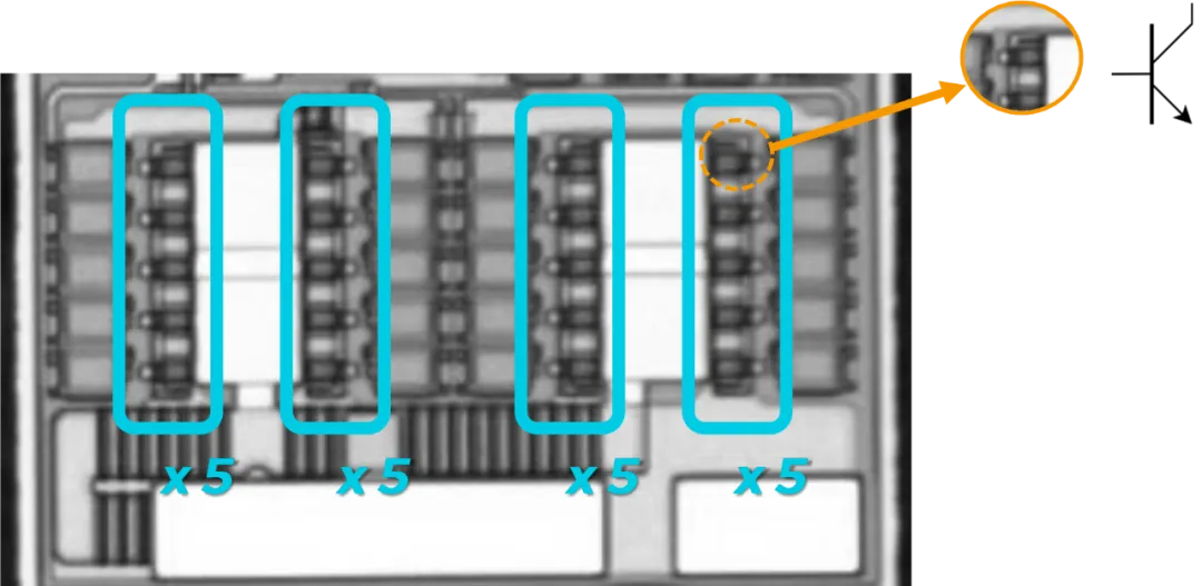
Figure: Typical PA power-stage layout
Design considerations for current combining:
- Keep each power array short to ensure currents add in phase.
- Maintain routing symmetry between arrays to preserve phase alignment during combining.
- Wide routing for current combining introduces parasitic capacitance, which must be managed.
Because it is simple and convenient, current combining is extensively used.
Voltage combining
Voltage combining raises the optimal output impedance, enabling lower matching loss when matching to the load. It is suitable when the supply voltage substantially exceeds device breakdown voltage or when low-voltage devices are stacked to form higher-voltage PA stages.
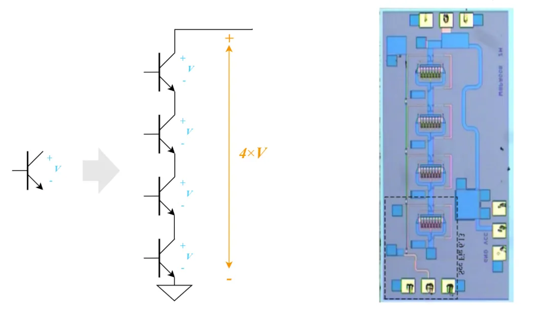
Figure: Typical circuit and implementation example using voltage combining
For example, GaAs HBT devices with VBCEO around 10–25 V are typically biased below 5 V. Around 2016, some vendors experimented with boosting battery voltage to around 11 V to supply cascode voltage-combined PAs to improve optimal output impedance and overall efficiency. That approach saw limited use in some flagship phones, but the need for an extra boost converter limited its general adoption.
Power combining
Some combining schemes do not fit neatly into current or voltage combining and are categorized as power combining. A common implementation uses power combiners such as the Wilkinson power combiner/divider. The Wilkinson combiner provides matchable three-port behavior and can be used to combine outputs of separately designed PAs.
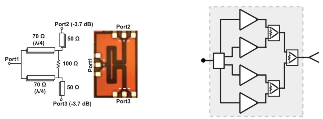
Figure: Typical Wilkinson combiner and a PA built around it
Wilkinson combiners require two quarter-wave transmission line sections and a 100 ohm resistor between branches, which increases area. For area-constrained designs, direct binary combining is often used instead, trading perfect three-port matching for reduced area and simpler layout. Transformers or spatial combining methods have also been used for power combining.
Special power combining
Special combining methods incorporate additional design features during power combining to realize complex behaviors. Common special combining methods include push-pull, balance, and Doherty.
Push-pull PA
Push-pull PAs combine two amplifiers that conduct on opposite halves of the waveform. Each PA transistor can be biased in a high-efficiency mode such as Class B, giving the combined amplifier higher overall efficiency. A push-pull pair may use complementary NPN/PNP devices or two NPN devices with a balun to create differential drive and virtual reference points.
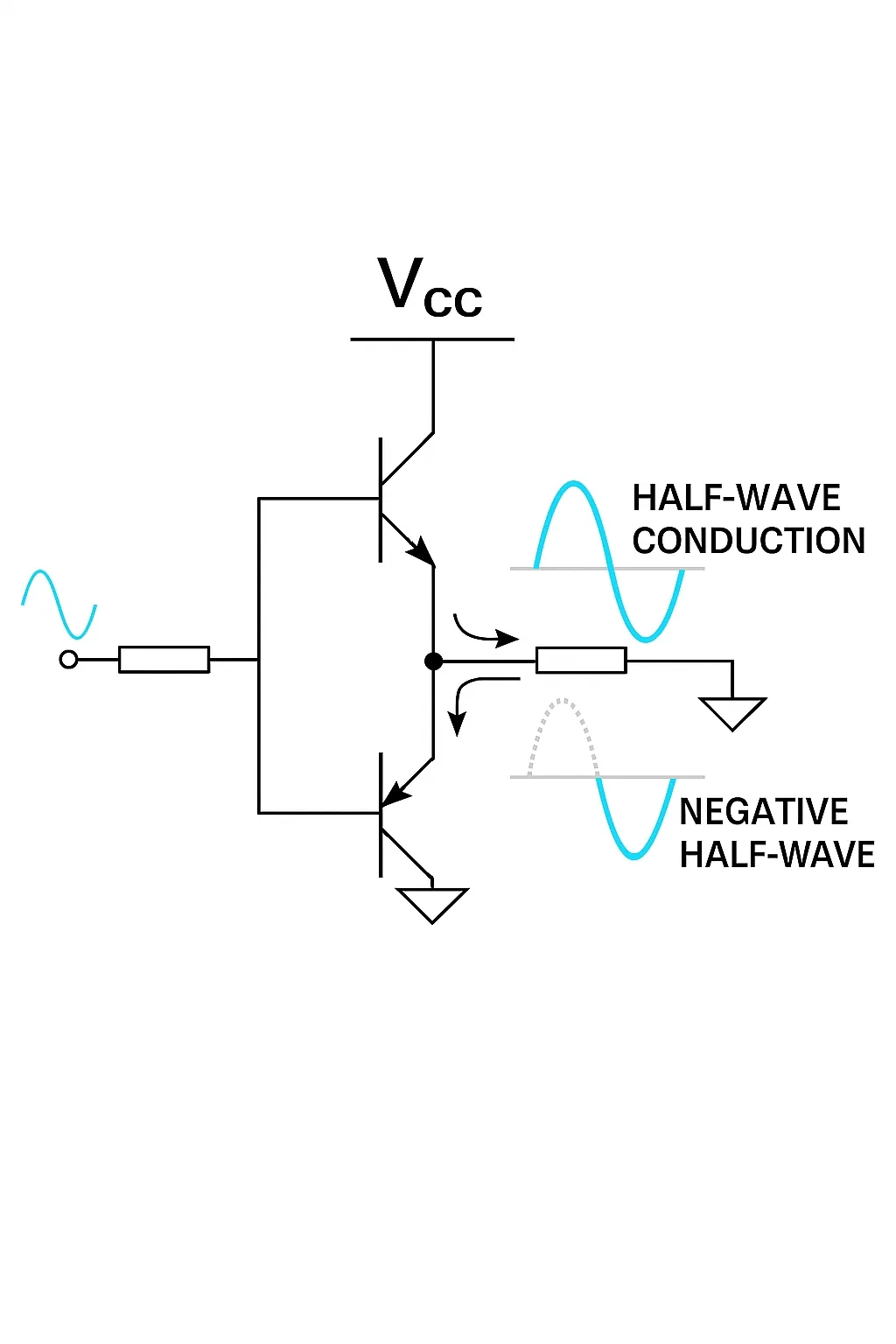
Figure: Push-pull PA schematic
In integrated implementations where PNP devices are less feasible, two NPNs are driven in antiphase by a balun. In that case, RF currents flow differentially between the two paths with the midpoint acting as a virtual reference.
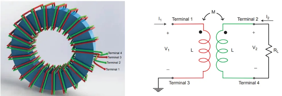
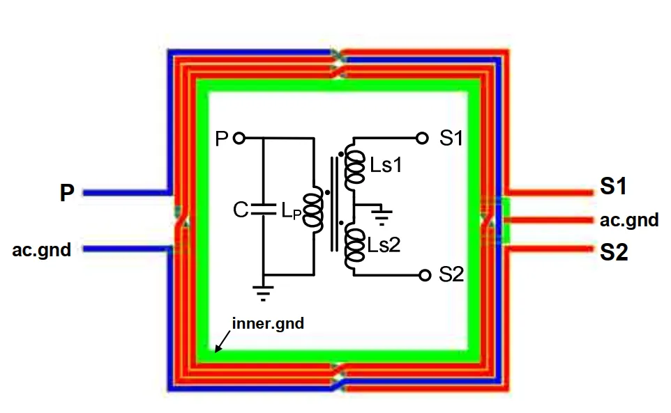
Push-pull PAs can also combine two Class A devices to increase output power rather than improve efficiency. Baluns, which convert between single-ended and differential signals, are essential in push-pull designs. Baluns are commonly implemented as dual-winding transformers or as coupled metal traces in ICs using edge or broadside coupling. Transformer baluns can also provide impedance transformation.
Design cues for identifying push-pull PAs:
- Two symmetric PA paths.
- Symmetric balun windings before/after the PA paths.
Balance PA
Balance PA, or balanced amplifier, also uses two PA paths but differs from push-pull in that it employs 90° power split and recombine networks. If the two paths are perfectly symmetric, reflected signals cancel at the input and output ports, improving VSWR over a certain bandwidth. This makes balance PAs suitable where improved S11/S22 is required.
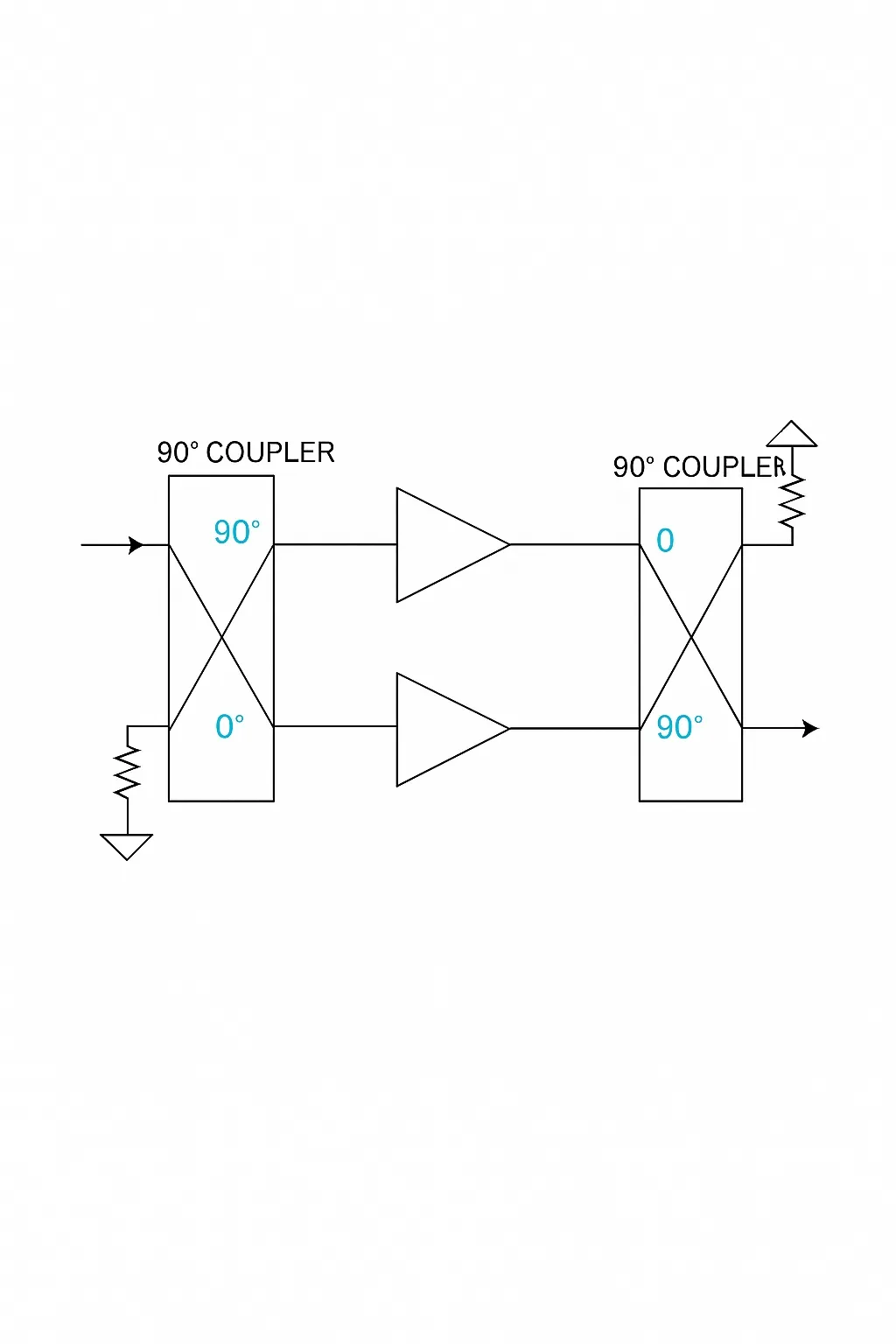
Figure: Balanced PA block diagram
Reflection cancellation in a balanced PA yields improved input and output match around the design frequency. For example, a balanced design centered at 1.5 GHz can improve S22 from -10 dB to -35 dB around the center frequency and maintain S22 below -15 dB across 1.4–1.6 GHz.
However, the balanced PA relies on an accurate 90° phase shift, and the coupler’s phase accuracy is frequency dependent. Thus, balanced PA performance is effective only within a limited band. Outside that band, S11/S22 and S21 can degrade compared with single-ended designs.
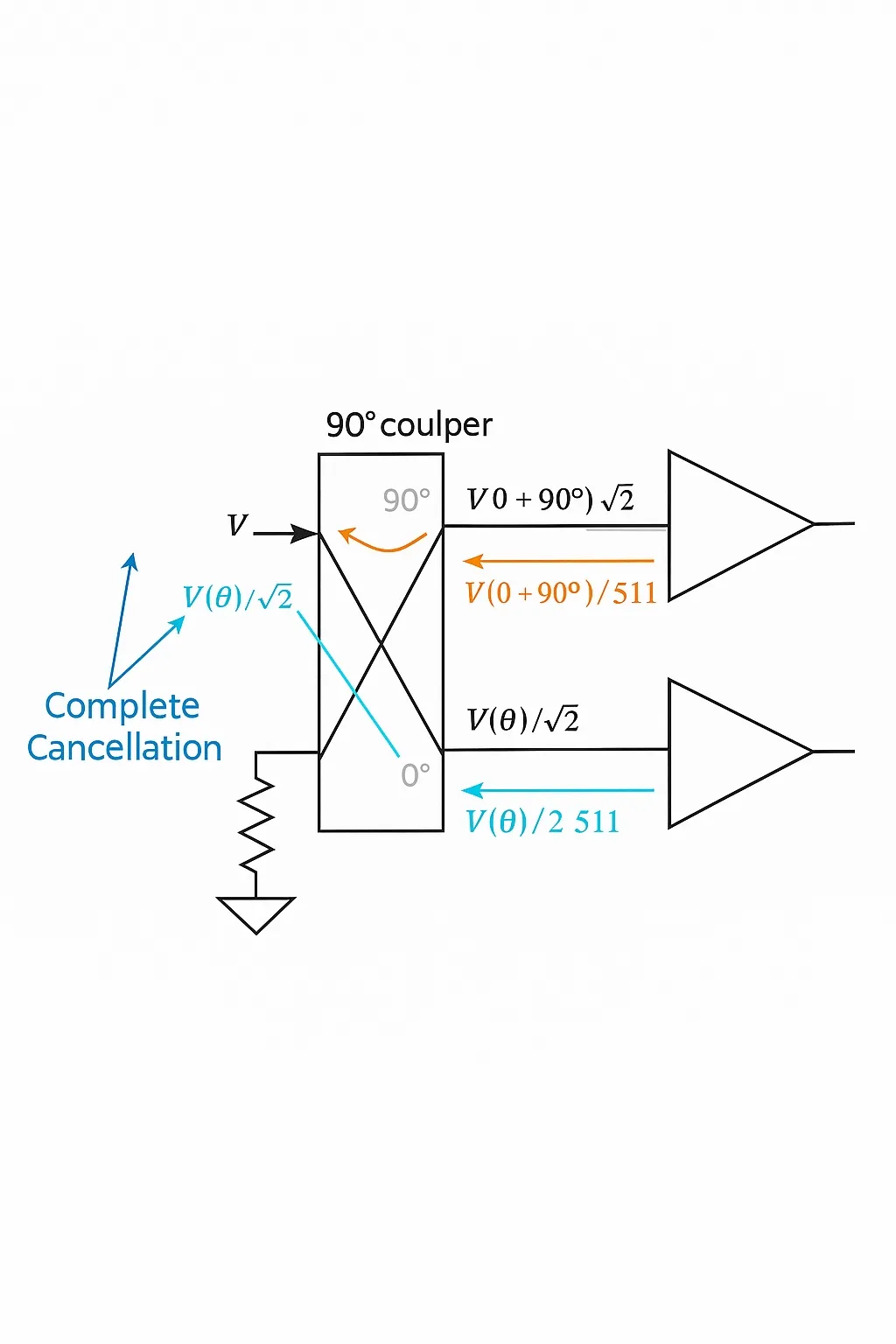
Figure: How balanced amplifiers improve input VSWR
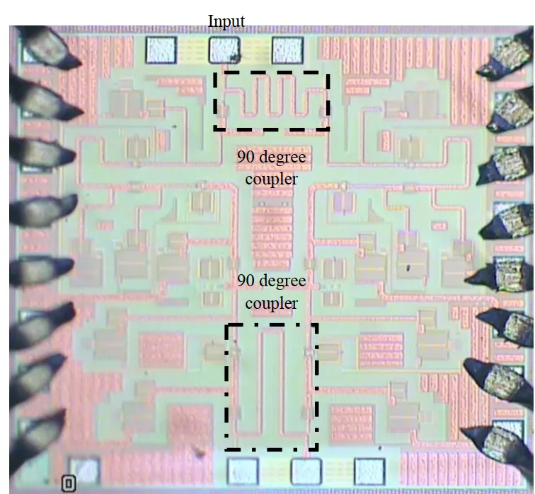
Because of its load-insensitive behavior near the cancellation point, balance PA is sometimes called Load Insensitive PA or LIPA. Implementations of the 90° split/combiner include phase shifters, directional couplers, or quadrature hybrid networks. At microwave and mmWave frequencies, distributed couplers/hybrids are commonly used to realize the required 90° phase shift.
Design cues for identifying balance PAs:
- Two symmetric PA paths.
- An asymmetric power split/combining network implementing a 90° phase difference.
- Improved S11/S22 near the cancellation frequency.
Doherty PA
Doherty PAs have attracted significant attention in mobile RF PA design due to their improved efficiency, especially during power backoff. The Doherty concept leverages dynamic load modulation: two amplifiers operating in different states cooperate so that the effective load seen by the main amplifier changes with output level, improving backoff efficiency.
Doherty architecture is not new. William H. Doherty of Bell Labs invented it in 1936 to build efficient high-power transmitters. The technology found increased relevance from the 1990s onward with mobile communications and advanced semiconductor and linearization techniques, becoming widespread in base station PAs.
The fundamental principle of Doherty PA is load modulation. If a load R is driven by a voltage source V1 and a current source I2, the impedance seen by V1 depends on I2. Varying I2 therefore modulates the load impedance seen by V1, which is the essence of load modulation.
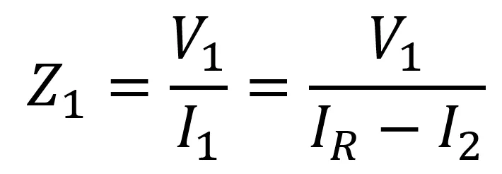
Figure: Load modulation under voltage and current source excitation
In PA implementations, transistors are often modeled as current sources. Doherty designs use impedance inverter networks to translate current-source behavior into the required voltage behavior and include compensation lines for phase alignment and matching.
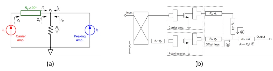
Figure: Doherty principle and implementation
A Doherty PA contains a Carrier path and a Peak path. At low power only the Carrier is active and sees a high load impedance for high efficiency. At high power the Peak amplifier turns on, modulating the Carrier load to achieve higher output power while maintaining efficiency across power backoff.
In practice, Doherty analysis requires simultaneous consideration of power, voltage, and impedance. Designers analyze two operating points—backoff power and saturation power—and study how each transistor’s impedance, power, and voltage change between those points.
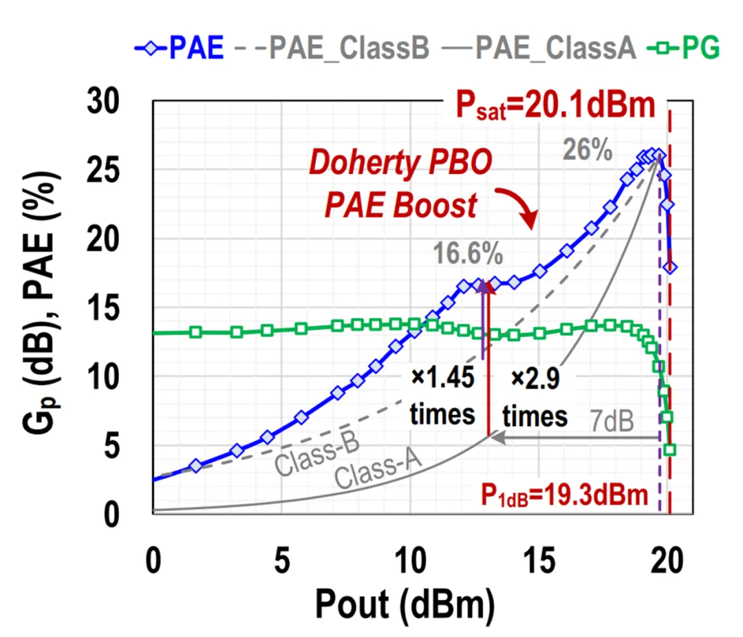
Figure: Doherty efficiency improvement during power backoff (example: 60 GHz PA)
Doherty PAs are common in base stations but less so in handsets. Mobile devices operate in complex environments with many bands and modes, and Doherty’s load sensitivity and narrower bandwidth can complicate handset integration. To use Doherty in phones, designers often sacrifice some backoff efficiency to meet temperature, antenna VSWR, and multi-band requirements.
Design cues for identifying Doherty PAs:
- At least two amplifier paths.
- Asymmetry between the paths, either by design or biasing.
- Non-symmetric power combining network.
- Distinctive S11/S22 behavior that differentiates it from balance PAs.
Hybrid and combined architectures
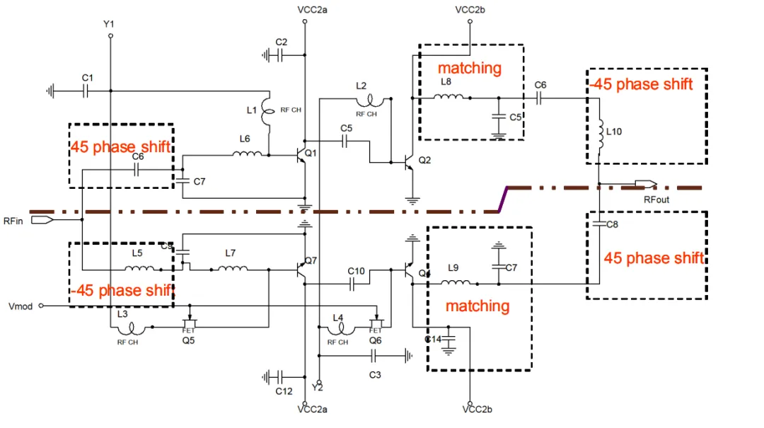
PA architectures can be mixed. For example, within a Doherty or push-pull PA each amplifier branch can use current or voltage combining. Different special combining techniques can be combined: a Doherty carrier and peak amplifier could each be push-pull devices, or two Doherty PAs could be combined into a balanced arrangement to reduce load sensitivity. Hybrid designs may use Wilkinson splitters, quadrature couplers, differential amplifiers, and Doherty topology together.
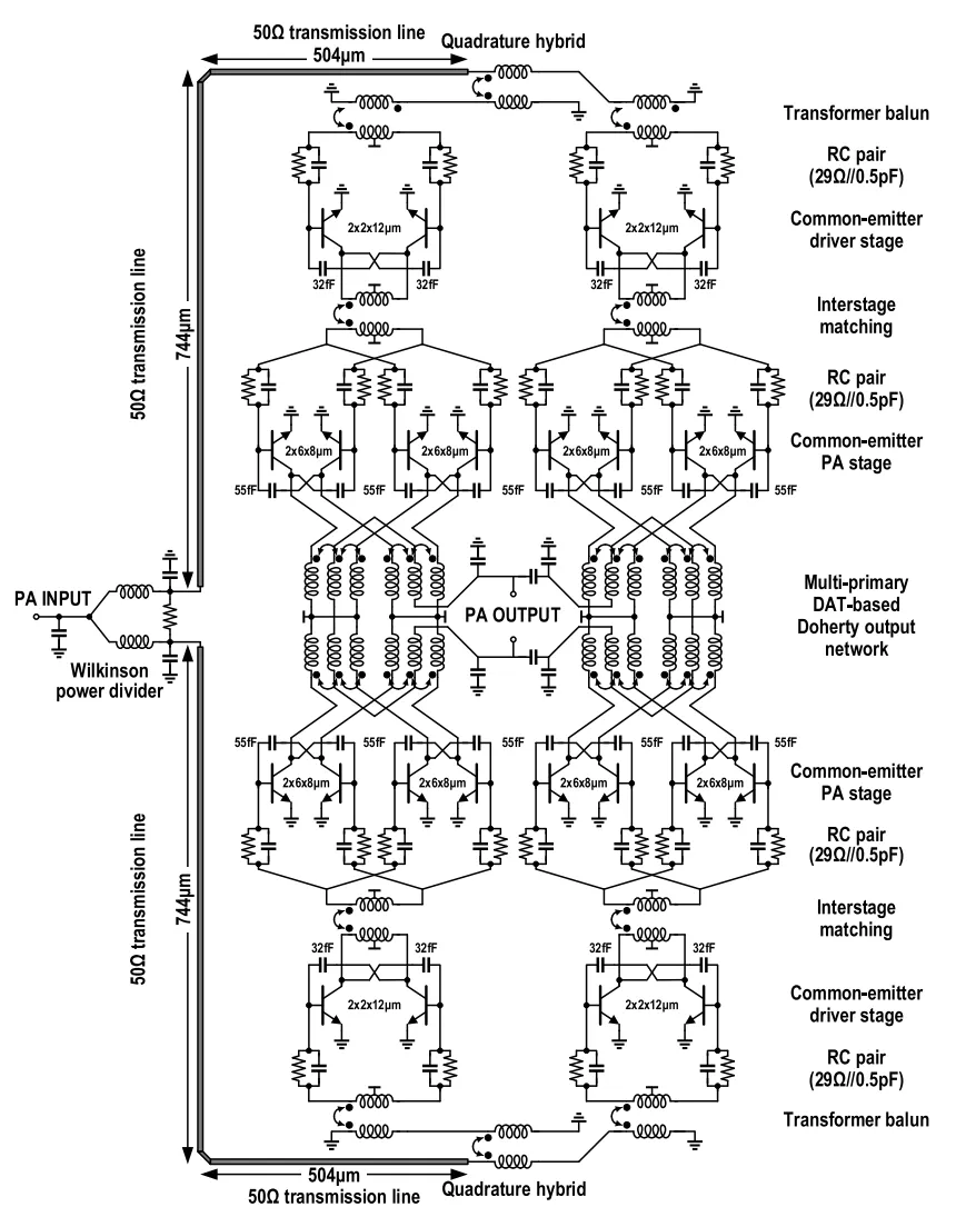
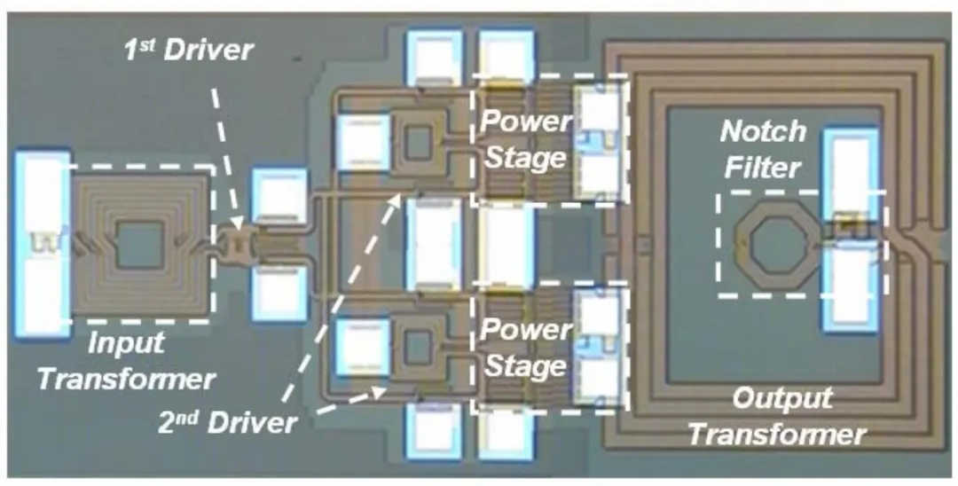
Figure: Example PA combining multiple architectures
Conclusion
This article summarized common PA architectures used in engineering practice, explaining design principles, architecture characteristics, and typical implementation methods. There is no universally best PA architecture; the right choice depends on system requirements and constraints. Understanding the characteristics of different PA types is essential for selecting a suitable architecture.