ALLPCB


Abstract
This article proposes a 5G millimeter-wave active array package antenna. The array consists of an 8x16 microstrip antenna element arrangement and uses a coupled differential feed to achieve wideband matching and a highly symmetric radiation pattern. By arranging the antenna and the beamforming chips carefully, feedline loss from the chip RF ports to the antenna subarrays is reduced, improving the overall efficiency of the active array antenna. Measured results show that the array achieves an equivalent isotropically radiated power (EIRP) greater than 60 dBm across the 24.25–27.5 GHz band. Gain reduction when scanning the array beam to +/-30 deg and +/-60 deg is no more than 0.6 dB and 4.1 dB respectively, indicating good wide-angle beam scanning performance.
Introduction
5G mobile communication technologies can provide higher user data rates, lower latency, and very large numbers of connected wireless devices. Compared with the already commercialized sub-6 GHz bands, the millimeter-wave bands offer abundant spectrum resources suitable for high-bandwidth hotspot applications. Moreover, the low-latency characteristics of millimeter-wave communication facilitate industrial networking applications, improving manufacturing efficiency and product reliability.
In 5G millimeter-wave systems, the design of large-scale phased-array antennas and the integrated packaging of package antennas with chips are two key technologies. On one hand, large-scale phased arrays in the millimeter-wave band provide a suitable solution for high-rate, low-latency, and robust links between base stations and mobile devices. On the other hand, antenna and feed-network losses in the millimeter-wave band are non-negligible; traditional separated antennas require long feedline electrical lengths, introducing unnecessary loss. The package antenna (AiP) approach can increase delivered circuit power, reduce path loss, and improve electromagnetic reliability of the antenna system.
Initial work on integrating antennas into packages was proposed by research groups at Nanyang Technological University and Georgia Tech in 2001. In 2018 Professor Rebeiz's team at UC San Diego reported a single-polarization phased-array transceiver for 5G millimeter-wave communications with 64 antenna elements and +/-50 deg scanning in the H-plane, achieving an EIRP of 52 dBm. In 2019 a Japanese electrical company designed a phased-array package antenna for 5G NR using eight package antenna elements capable of +/-50 deg scanning.
Moreover, many researchers in China have proposed phased-array antenna designs, though their performance still has room for improvement. Against this background, this article presents a 5G millimeter-wave active array package antenna featuring wide-angle scanning and low cross-polarization. The array uses a one-drive-two-antenna subarray layout to reduce the number of chips required. A multi-layer PCB process integrates the antenna and chips into a single package, lowering manufacturing cost. The large-scale packaged array and beamforming chips enable high gain and +/-60 deg wide-angle scanning in the azimuth plane, demonstrating promising application potential.
1 Subarray design
1.1 Subarray structure
The proposed design is an 8x16 active array package antenna operating in the 5G millimeter-wave band from 24.25 to 27.5 GHz, with gain greater than 24 dBi and beam scanning of +/-60 deg in the horizontal plane and +/-15 deg in the vertical plane. This section first addresses the design of a wideband, wide-beam subarray. To meet the array scanning requirements while minimizing the number of beamforming chips and simplifying routing, a one-drive-two-antenna subarray layout is adopted.
Figure 1(a) shows a 3D exploded view of the one-drive-two-antenna subarray. To improve structural and pattern symmetry and ensure symmetric scanning coverage for +/-60 deg, a differential feed scheme is used at the antenna element feed. In Figure 1(b) the blue S-shaped lines are the differential feed network; they implement a 180-degree phase difference between the two outputs using half-wavelength extension lines, and they connect to two feed vias for differential excitation of the microstrip antenna. The inputs of the differential feeds connect to a T-type power divider with two output ports; the divider input provides the simulation excitation port. Both feed vias connect to the first PCB layer and are coupled to 45-degree oriented square patches on that layer. Compared with direct probe-fed vias, the coupling feed introduces an equivalent capacitance that can partly cancel the equivalent inductance of relatively long vertical vias, thereby widening the antenna impedance bandwidth.
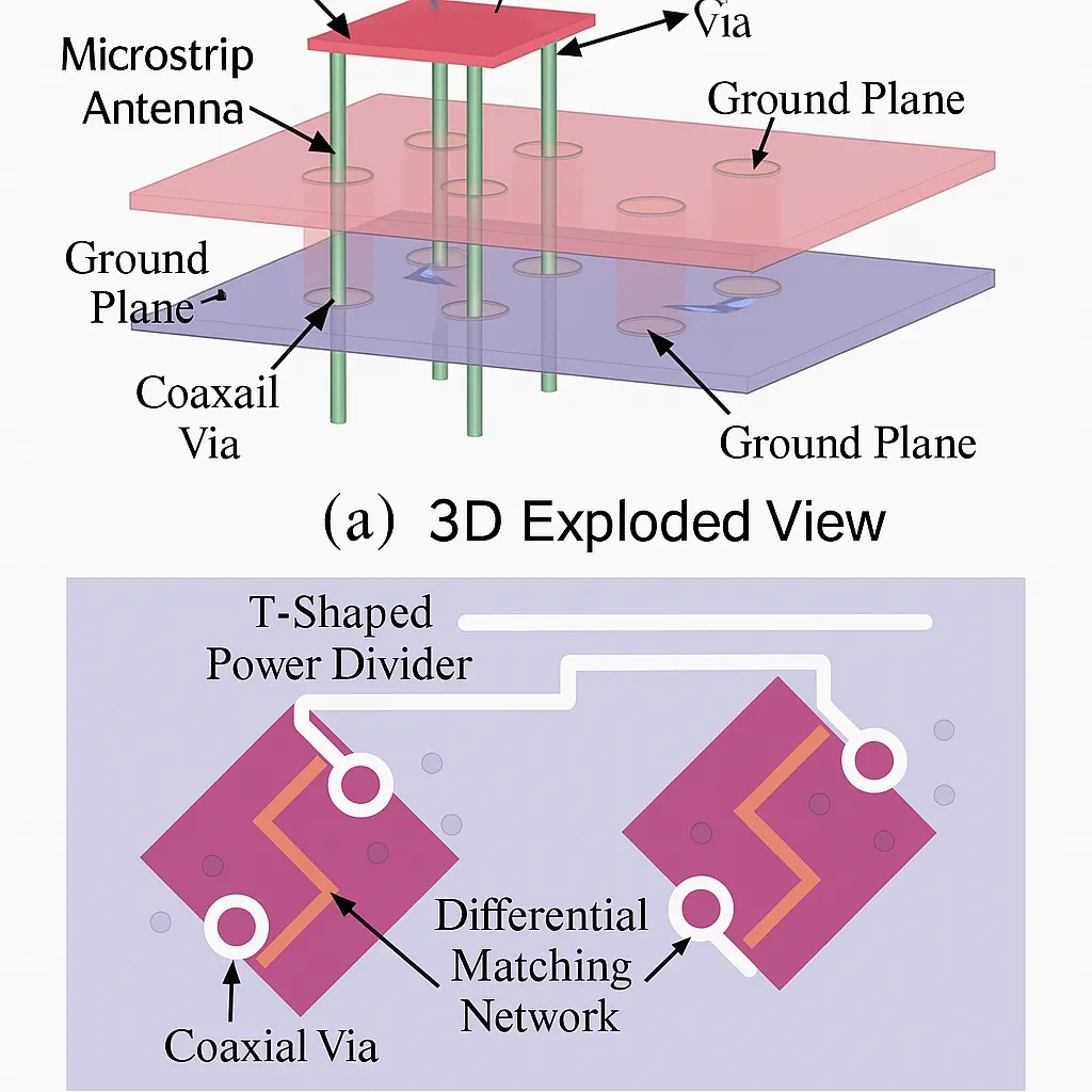
Figure 1 3D exploded view and top view of the one-drive-two-antenna subarray
1.2 Subarray performance and analysis
Simulating the one-drive-two-antenna subarray under master-slave boundary conditions effectively models the radiation performance of subarrays in a large-scale array. Figure 2 shows the simulated results after parameter optimization. The subarray achieves S11 < -15 dB across 24.25–27.5 GHz, and the peak gain is approximately 6–7 dBi.
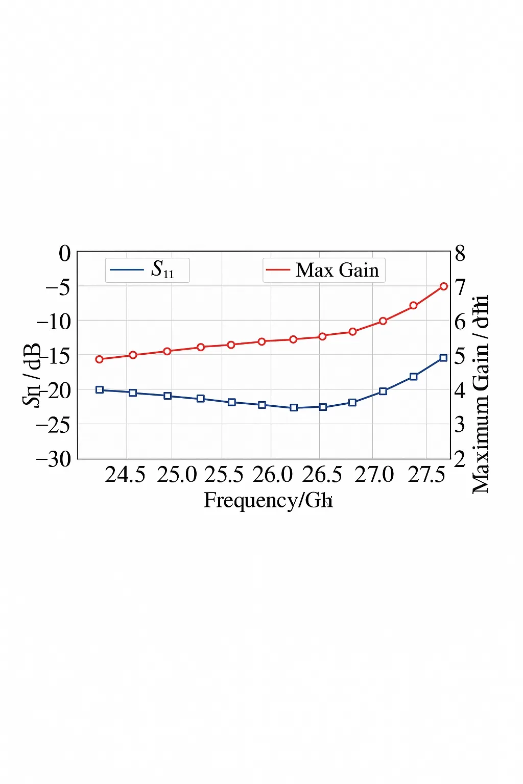
Figure 2 S11 and maximum gain of the element under master-slave boundary conditions
Figure 3 shows the simulated radiation patterns of the subarray under master-slave boundary conditions. In the horizontal plane the 3 dB beamwidth is about 90 deg and the 6 dB beamwidth about 130 deg; therefore an 8x16 array composed of this subarray can achieve gain reduction of no more than 6 dB when scanning +/-60 deg. In the vertical plane the 3 dB beamwidth is about 58 deg; gain reduction at 15 deg is no more than 1 dB, so the array can achieve vertical scanning of +/-15 deg with gain reduction within 1 dB.
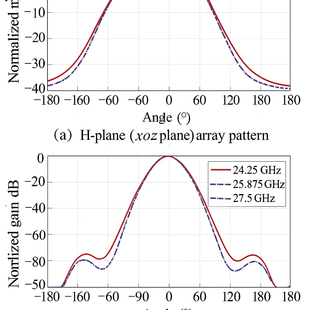
Figure 3 Simulated subarray radiation patterns under master-slave boundary conditions
2 Feed network design for the array antenna
2.1 Overall architecture of the active array antenna
The designed 8x16 active array antenna includes the 8x16 antenna array, beamforming chips that control feed amplitude and phase for each subarray, a 1-to-16 Wilkinson power divider, and front-end transceiver modules. Figure 4 shows the RF-end architecture of the 8x16 active array. Each beamforming chip has four transceiver channels, each connected to the feed lines of four one-drive-two-antenna subarrays. The chip can independently control amplitude and phase on each channel to steer the array beam, adjust gain, control sidelobe level, and set EIRP. Each chip's RF interface is combined via a 1-to-16 Wilkinson power divider into a single RF port. Compared with large chips with many channels (16 or 32 channels), the architecture in Figure 4 places chips closer to their antenna subarrays, reducing feedline loss per chip channel and improving feedline symmetry. This reduces per-channel phase error and improves system consistency and stability.
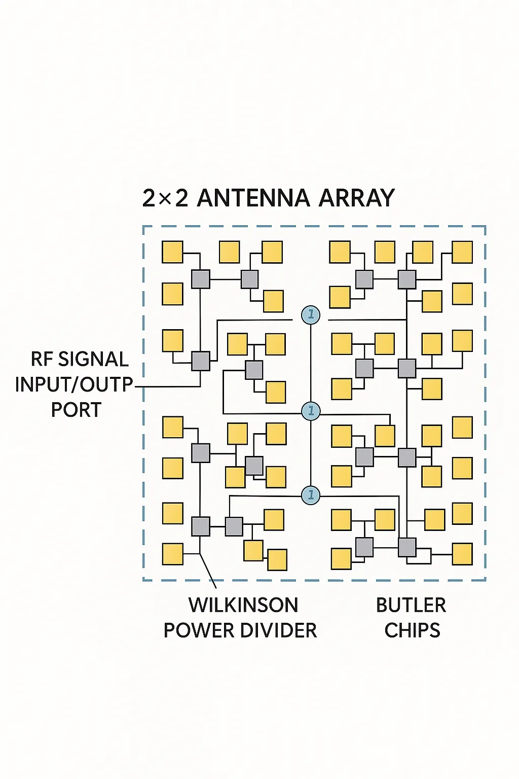
Figure 4 RF-end architecture of the 8x16 active array antenna
2.2 Design of the 1-to-16 Wilkinson power divider
Figure 5 shows the model of the 1-to-16 power divider. The basic unit is a 1-to-2 Wilkinson divider with a 100 ohm isolation resistor between the two output ports. Input and output impedances are 50 ohm. Blue traces are routed on the PCB bottom metal layer as ground coplanar waveguide (GCPW) structures; red traces are on the PCB third-from-top layer as packaged stripline. Layer transitions between blue and red traces are implemented with quasi-coaxial vertical vias, as illustrated in Figure 6. Symmetric grounding vias are placed along both sides of the traces to avoid parallel-plate modes and reduce insertion loss of the divider.
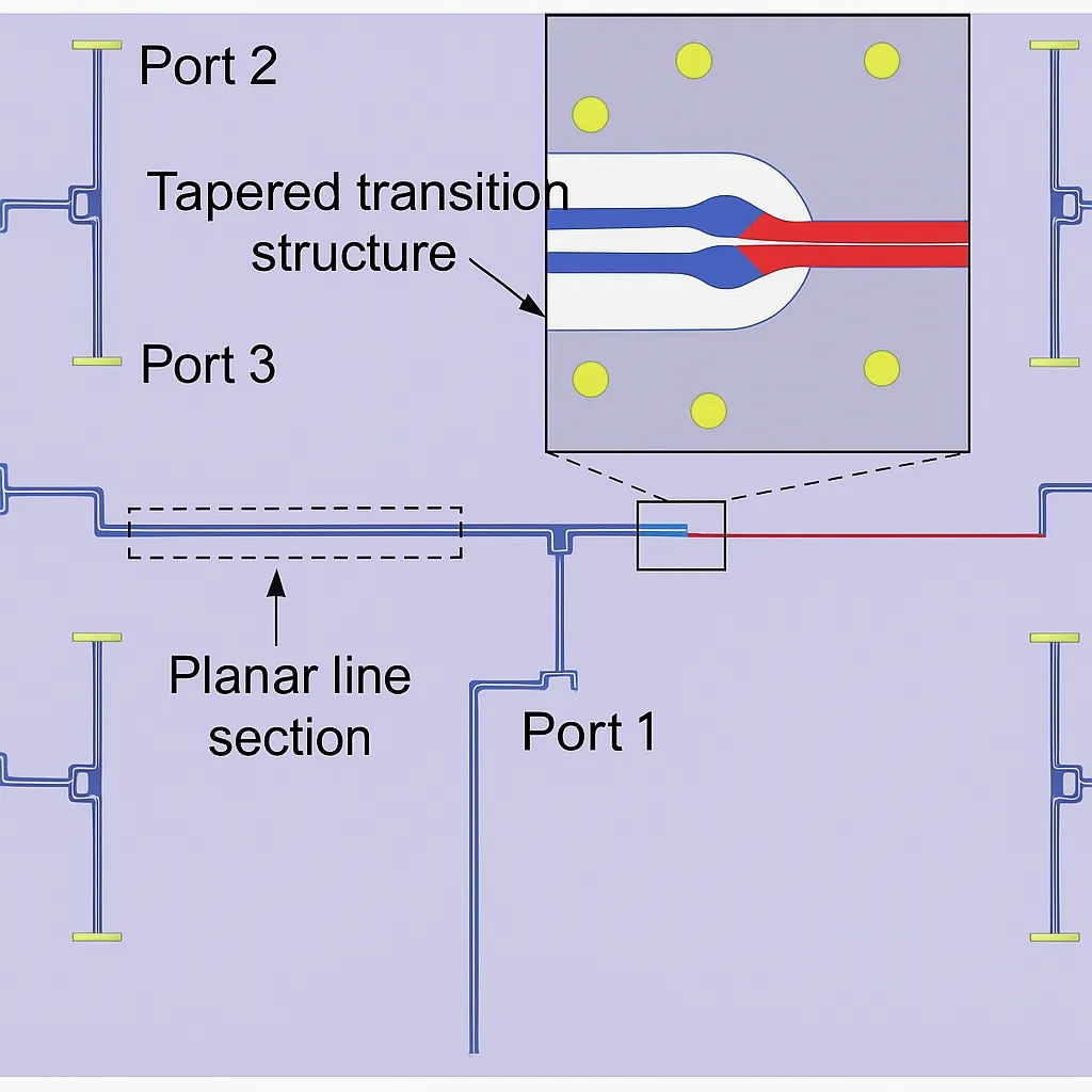
Figure 5 1-to-16 power divider model for the 8x16 active array antenna
Figure 6 Layer stack illustration of the array package antenna feed network
Figure 7 presents simulation results for the 1-to-16 divider, where ports 1, 2, and 3 correspond to the labeled ports in Figure 5. The divider input reflection coefficient (port 1) is below -15 dB; output port reflection coefficients (port 2) are below -20 dB. By symmetry port 3 shows the same reflection. The insertion loss (S21) of the 1-to-16 divider is about 13.4 dB, which is 1.4 dB higher than the theoretical ideal 12 dB due to conductor loss, dielectric loss, and losses from layer transitions. Isolation between adjacent output ports 2 and 3 (S23) is greater than 20 dB, indicating good isolation performance.
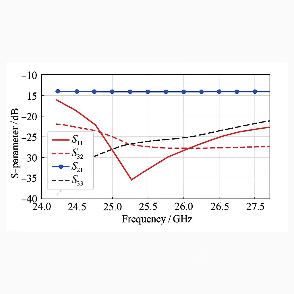
Figure 7 Simulation results of the 1-to-16 power divider for the 8x16 active array antenna
3 Implementation and testing of the active array antenna
3.1 Simulation of the 8x16 array antenna
Based on the simulated element design, a full 8x16 array performance verification was conducted using the Finite Array module in ANSYS HFSS. Figure 8 shows the finite-array simulation model, expanding the one-drive-two-antenna subarray into an 8x16 array.
Figure 8 8x16 array model used for Finite Array simulation
First, the array performance without beam steering was analyzed. Figure 9 shows the Smith chart and rectangular plots of the active reflection coefficients for several elements when the beam points at theta0 = 0 deg; these include elements at the array center, array corner, and near the corner. Center and near-corner elements exhibit active reflection coefficients consistent with the master-slave boundary simulations, indicating that most elements in the 8x16 array experience a similar surrounding boundary environment to that of an infinite array. A few corner elements show increased active reflection coefficients due to edge effects; in general, elements closer to the edge have larger increases. Overall, active reflection coefficients for all elements are below -10 dB, meeting design requirements.
Figure 11 shows the array gain and 3 dB beamwidths in the horizontal and vertical planes when the beam points at theta0 = 0 deg. The array gain across 24.25–27.5 GHz is 23.9–24.9 dBi, consistent with the array gain estimated from the active element patterns. The 3 dB beamwidth in the horizontal plane (phi = 0 deg) is 12.5–14.2 deg, and in the vertical plane (phi = 90 deg) is 7–8 deg.
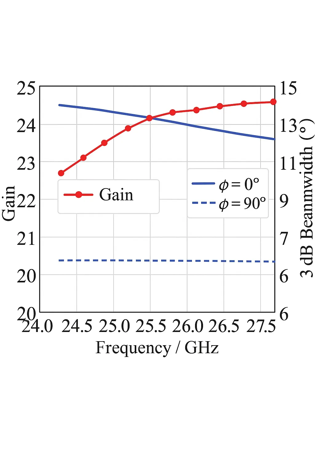
Figure 11 Array gain and 3 dB beamwidths for the 8x16 array when not scanning
Figure 12 shows the horizontal-plane radiation patterns for 0 to 60 deg scanning at the center frequency. When steering to 15 deg and 30 deg, gain reduction is minimal, under 1 dB, and sidelobe levels are around -13 dB. At 45 deg scanning, gain reduction is under 3 dB with sidelobe levels around -13 dB. At 60 deg scanning, gain reduction is around 5 dB, consistent with estimates from active element patterns. The sidelobe level at 60 deg is slightly higher, about -8 dB. In summary, the array demonstrates good wide-angle beam scanning performance with relatively low sidelobe levels.
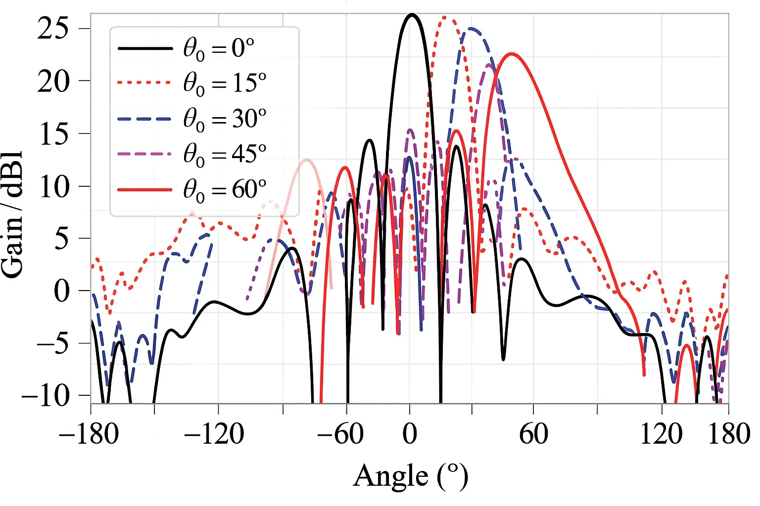
Figure 12 0–60 deg scanning radiation patterns of the 8x16 array at center frequency 25.875 GHz
3.2 Testing and analysis of the active array antenna
A prototype was fabricated based on the above design, integrating control circuitry, signal processing, beamforming chips, and the large-scale array. The prototype was tested in a millimeter-wave anechoic chamber. Figure 13 shows the prototype and the chamber test setup, and Figure 14 illustrates the antenna test method. Measured results indicate the antenna achieves an EIRP greater than 60 dBm.
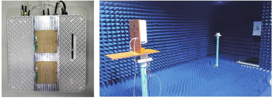
Figure 13 Prototype of the active array antenna and anechoic chamber test environment
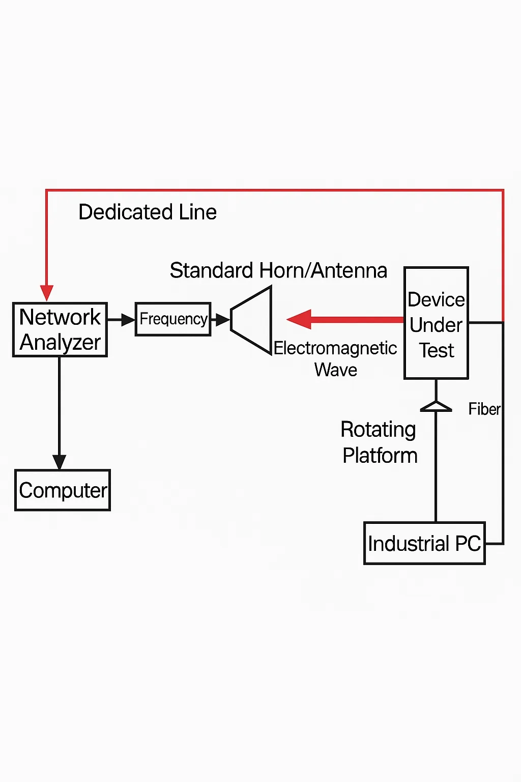
Figure 14 Schematic of the antenna test method
Figure 15 shows the measured horizontal-plane 0–60 deg beam scanning patterns at the center frequency of 25.875 GHz. When scanning to 10 deg the gain is highest and slightly exceeds the no-scan gain, likely due to mutual coupling among elements causing small variations in the active element pattern and shifting the maximum gain direction. At 30 deg scanning the sidelobe level is near -10 dB and gain reduction is less than 0.6 dB. At 60 deg scanning the gain reduction is no more than 4.1 dB, demonstrating that the active array maintains low gain degradation at large scan angles and has good wide-angle scanning performance.
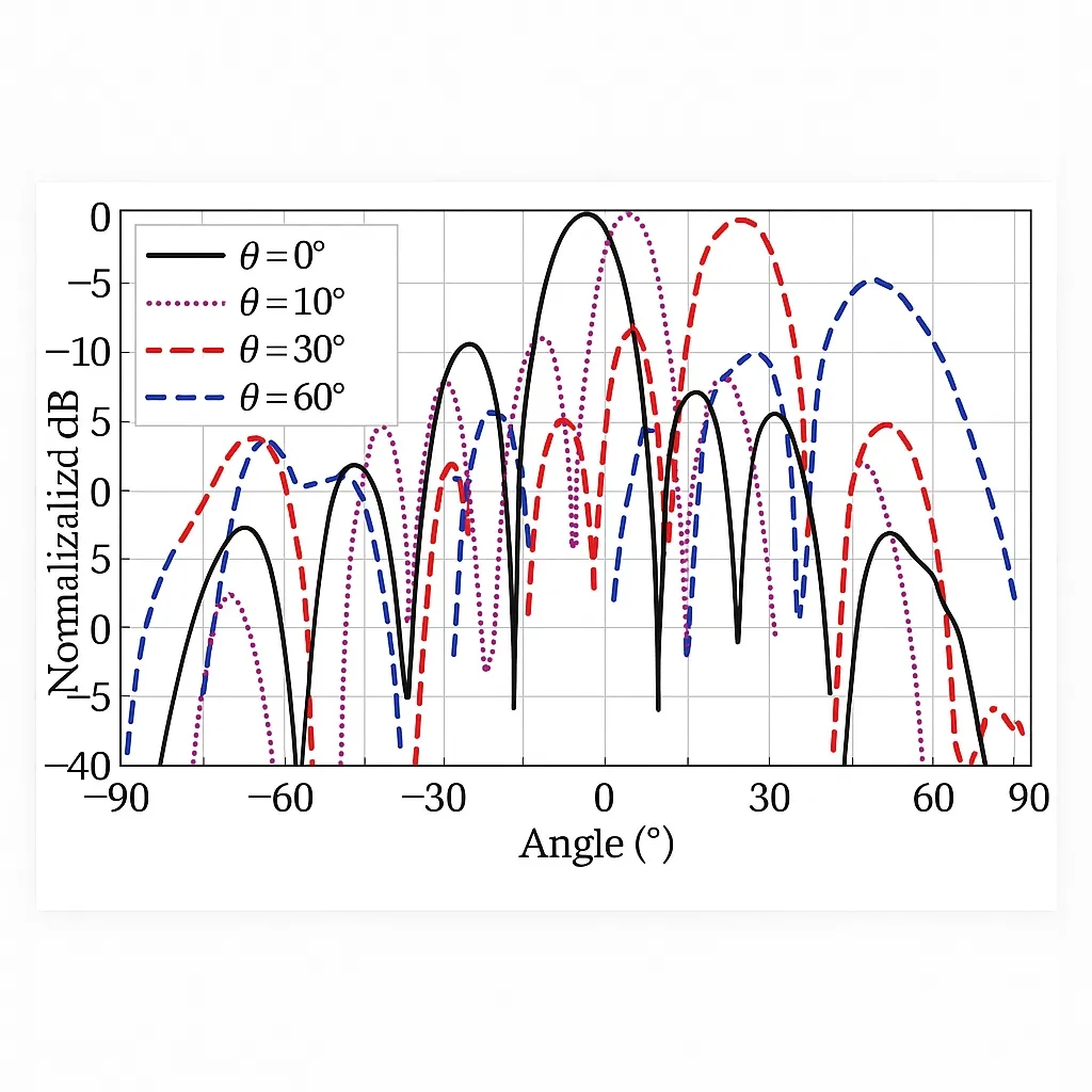
Figure 15 Horizontal-plane beam scanning patterns (measured)
Figure 16 shows the measured vertical-plane 0–15 deg beam scanning patterns at the center frequency of 25.875 GHz. In the vertical plane, sidelobe levels are below -10 dB for 0–15 deg scanning, and gain reduction at 15 deg is no more than 1.5 dB, indicating good wide-angle scanning performance in the vertical plane as well.
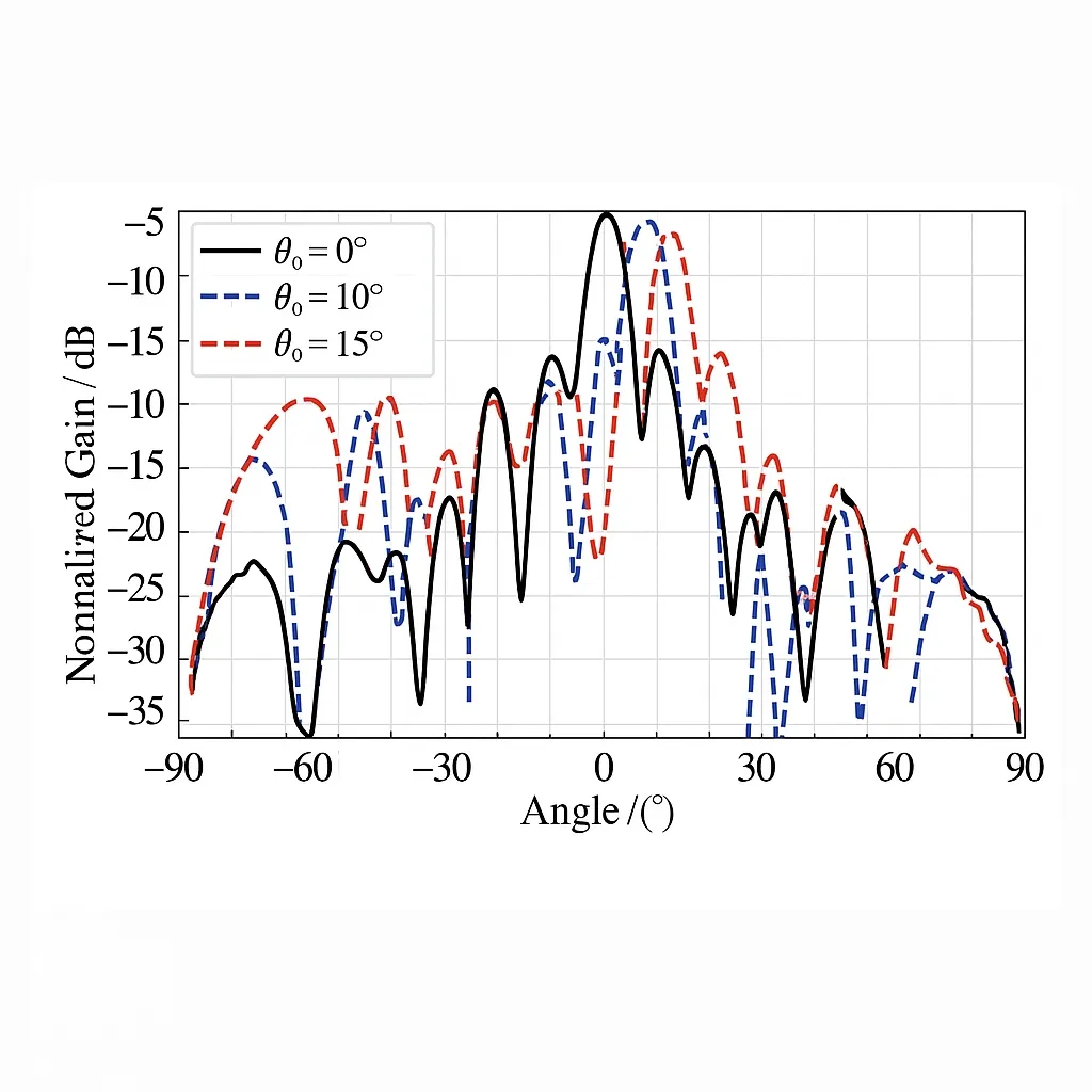
Figure 16 Vertical-plane beam scanning patterns (measured)
Conclusion
This work completed simulation, fabrication, and testing of an 8x16 active array package antenna based on a one-drive-two-antenna subarray. The coupled differential-fed microstrip antenna structure achieves wide bandwidth, wide beam, and symmetric patterns. A Wilkinson-based feed network ensures good amplitude and phase consistency at the beamforming chip combiner ports, supporting the array's performance. Measured results show that with beamforming chip amplitude/phase control, the active array provides +/-60 deg horizontal and +/-15 deg vertical scanning and an EIRP above 60 dBm. The proposed 5G millimeter-wave active array package antenna demonstrates strong performance for 5G mobile communication applications.