 ALLPCB


If you're diving into the world of multi-layer PCB manufacturing, understanding fabrication drawings is crucial. These drawings are the blueprint that guides the production of your printed circuit board (PCB), ensuring every layer, trace, and component is placed with precision. In this comprehensive guide, we’ll break down what fabrication drawings are, why they matter for multi-layer PCB design, and how to create and interpret them effectively for successful manufacturing.
Whether you're an engineer, designer, or hobbyist working on complex electronics, this blog will walk you through the essentials of fabrication drawings for multi-layer PCB manufacturing, focusing on the long-tail keyword "PCB design fabrication multilayer." Let’s explore the details step by step to help you achieve flawless results in your projects.
What Are Fabrication Drawings in Multi-Layer PCB Manufacturing?
Fabrication drawings are detailed technical documents that communicate the design and manufacturing requirements of a PCB to the production team. For multi-layer PCBs, which consist of multiple layers of conductive copper separated by insulating materials, these drawings are even more critical. They provide a visual and numerical representation of the board’s structure, including layer stack-up, dimensions, drill holes, and material specifications.
Unlike a schematic, which focuses on the electrical connections, fabrication drawings are all about the physical construction of the board. They ensure that the manufacturer can replicate your design accurately, avoiding costly errors during production. For multi-layer PCBs, where signal integrity and impedance control are vital, these drawings must be precise to maintain performance standards.
Key Components of Fabrication Drawings
Fabrication drawings for multi-layer PCBs typically include the following elements:
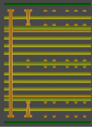
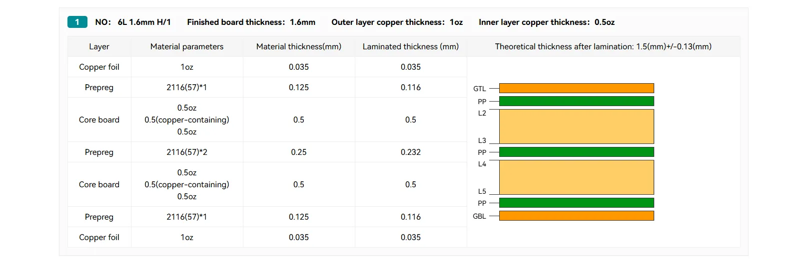
- Layer Stack-Up Diagram: Shows the arrangement of copper layers and insulating materials, often with details on thickness (e.g., 1.6mm total board thickness).
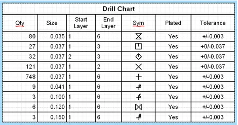
- Drill Chart: Lists the sizes and locations of holes for vias and through-hole components, with tolerances like ±0.05mm for precision.
- Dimensioned Layout: Provides exact measurements of the board outline and critical features.
- Material Specifications: Defines the type of substrate (e.g., FR-4) and copper weight (e.g., 1 oz/ft2).
- Notes and Tolerances: Includes specific instructions for manufacturing, such as impedance control targets (e.g., 50 ohms for high-speed signals).
Why Fabrication Drawings Matter for Multi-Layer PCB Design
Multi-layer PCBs are used in advanced electronics where space is limited, and performance is critical—think smartphones, medical devices, and aerospace systems. With multiple layers (often 4, 8, or even 16), the complexity increases, making fabrication drawings indispensable for several reasons.
1. Ensuring Accuracy Across Multiple Layers
In a multi-layer PCB, each layer must align perfectly to maintain electrical connections through vias. A small misalignment can disrupt signal paths or cause short circuits. Fabrication drawings provide exact coordinates and tolerances to ensure that each layer is manufactured and assembled correctly.
2. Controlling Signal Integrity and Impedance
High-speed designs often require controlled impedance to prevent signal degradation. For instance, a trace on a 4-layer PCB might need to maintain 50-ohm impedance for data rates exceeding 1 Gbps. Fabrication drawings specify trace widths, spacing, and dielectric thickness to achieve these targets, guiding manufacturers to meet performance standards.
3. Avoiding Manufacturing Errors
Without clear drawings, manufacturers might misinterpret design intent, leading to issues like incorrect hole sizes or misplaced components. Fabrication drawings act as a universal language between designers and manufacturers, reducing the risk of costly rework.
How to Create Fabrication Drawings for Multi-Layer PCBs
Creating accurate fabrication drawings for multi-layer PCB manufacturing requires attention to detail and a solid understanding of both design and production processes. Below are the key steps to follow when preparing these documents for your "PCB design fabrication multilayer" project.
Step 1: Define the Layer Stack-Up
The layer stack-up is the foundation of a multi-layer PCB. It determines how many layers your board will have, the order of signal and ground planes, and the thickness of each dielectric layer. For example, a 6-layer PCB might include:
- Layer 1: Top signal layer
- Layer 2: Ground plane
- Layer 3: Inner signal layer
- Layer 4: Inner signal layer
- Layer 5: Power plane
- Layer 6: Bottom signal layer
Specify the thickness of each layer (e.g., 0.2mm for inner dielectrics) and the overall board thickness (e.g., 1.6mm). Include this information in a clear diagram within your fabrication drawing.
Step 2: Specify Drill and Via Details
Vias are critical in multi-layer PCBs for connecting different layers. Your fabrication drawing should include a drill chart that lists:
- Hole sizes (e.g., 0.3mm for microvias)
- Hole types (through-hole, blind, or buried vias)
- Tolerances (e.g., ±0.05mm)
- Locations using X-Y coordinates
Accurate via placement ensures reliable connections and prevents signal crosstalk in high-density designs.
Step 3: Include Dimensions and Tolerances
Provide precise measurements for the board outline, mounting holes, and any cutouts. Use standard tolerances, such as ±0.1mm for board dimensions, to account for manufacturing variations. Clearly label these dimensions on the drawing to avoid ambiguity.
Step 4: Add Material and Finish Specifications
Specify the materials to be used, such as FR-4 for the substrate and 1 oz copper for traces. Include details about the surface finish (e.g., HASL or ENIG) and solder mask color. These choices impact the board’s durability, thermal performance, and cost.
Step 5: Include Special Instructions
If your design requires specific manufacturing processes—like controlled impedance or embedded components—note these in the drawing. For example, you might specify that certain traces must maintain a 50-ohm impedance with a tolerance of ±10% to support high-speed signals.
Common Challenges in Fabrication Drawings for Multi-Layer PCBs
Even with careful planning, creating fabrication drawings for multi-layer PCBs can present challenges. Here are some common issues and how to address them during your "PCB design fabrication multilayer" process.
1. Miscommunication with Manufacturers
Different manufacturers may interpret drawings differently due to varying standards or tools. To minimize confusion, use industry-standard formats like Gerber files alongside your drawings. Include detailed notes to clarify any unique requirements.
2. Overlooking Impedance Control
Impedance mismatches can degrade signal quality in multi-layer designs. Always calculate the required trace width and spacing using tools or formulas based on the dielectric constant (e.g., 4.5 for FR-4) and desired impedance (e.g., 50 ohms). Document these values clearly in the drawing.
3. Incomplete Drill Information
Missing or incorrect drill data can lead to unusable boards. Double-check your drill chart for accuracy, ensuring all via types and sizes are accounted for. For instance, buried vias in a 12-layer PCB should be explicitly marked to avoid manufacturing errors.
Best Practices for Effective Fabrication Drawings
To streamline the multi-layer PCB manufacturing process, follow these best practices when preparing fabrication drawings:
- Use Standard Formats: Export drawings in widely accepted formats like PDF or DXF for compatibility with manufacturing systems.
- Label Everything Clearly: Ensure every element, from layers to tolerances, is labeled to prevent misinterpretation.
- Collaborate with Manufacturers Early: Share draft drawings with your manufacturing partner to identify potential issues before production begins.
- Validate with Software: Use PCB design software to simulate the stack-up and verify impedance values before finalizing drawings.
How Fabrication Drawings Impact Manufacturing Costs
The quality and clarity of your fabrication drawings can directly affect the cost of manufacturing multi-layer PCBs. Here’s how:
- Reduced Errors: Clear drawings minimize mistakes, saving time and money on rework. For example, a misdrilled via can scrap an entire batch of boards, costing hundreds of dollars.
- Optimized Materials: Specifying the right materials and thicknesses prevents over-engineering, which can inflate costs unnecessarily.
- Faster Turnaround: Well-documented drawings speed up the production process, as manufacturers spend less time clarifying details.
Tools for Creating Fabrication Drawings
Several software tools can help you create detailed fabrication drawings for multi-layer PCB manufacturing. These tools often integrate with design platforms to automate parts of the process:
- CAD Software: Tools like Altium Designer allow you to generate layer stack-up diagrams and drill charts directly from your design files.
- Gerber Viewers: Use these to review exported files and ensure all elements of the drawing are visible and accurate.
- Simulation Tools: Software for impedance calculation can help you define precise trace parameters for high-speed designs.
Conclusion: Mastering Fabrication Drawings for Multi-Layer PCB Success
Understanding and creating fabrication drawings is a fundamental skill for anyone involved in multi-layer PCB manufacturing. These drawings bridge the gap between design and production, ensuring that your complex, high-performance boards are built to specification. By focusing on details like layer stack-up, drill charts, and impedance control, you can avoid common pitfalls and achieve reliable results in your "PCB design fabrication multilayer" projects.
At ALLPCB, we’re committed to supporting engineers and designers with the resources and expertise needed for successful PCB manufacturing. Whether you’re working on a 4-layer board for a consumer device or a 16-layer design for industrial applications, mastering fabrication drawings will set you up for success. Take the time to refine your drawings, collaborate with your manufacturing partner, and leverage the right tools to bring your designs to life with precision and efficiency.


