 ALLPCB


If you're looking to understand through-hole PCB assembly, including its techniques like wave soldering, selective soldering, and manual soldering, as well as when to use it, you've come to the right place. Through-hole assembly is a traditional yet highly reliable method for mounting components on printed circuit boards (PCBs) by inserting leads through drilled holes and soldering them in place. It’s ideal for applications requiring durability, such as in power electronics or industrial equipment. In this comprehensive guide, we’ll dive deep into the through-hole assembly process, explore the types of through-hole components, and provide actionable tips to ensure successful implementation.
What Is Through-Hole PCB Assembly?
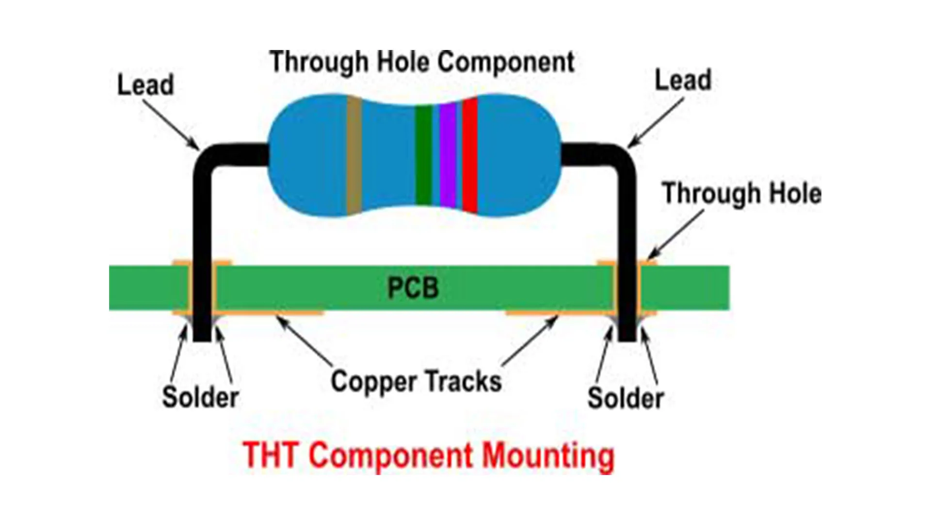
Through-hole PCB assembly, often abbreviated as PTH (plated through-hole) assembly, is a method of mounting electronic components onto a PCB. Unlike surface-mount technology (SMT), where components are placed directly on the board’s surface, through-hole assembly involves drilling holes in the PCB, inserting component leads through these holes, and soldering them on the opposite side. This creates a strong mechanical and electrical connection, making it a preferred choice for components that endure high stress or require long-term reliability.
The process has been a cornerstone of electronics manufacturing for decades due to its simplicity and robustness. While PCBA SMT has become more popular for compact designs, through-hole assembly remains relevant in specific applications. Let’s explore why and how it’s done.
When to Use Through-Hole PCB Assembly
Knowing when to opt for through-hole assembly over other methods is crucial for designing reliable and cost-effective electronics. Here are the primary scenarios where through-hole technology shines:
- High Mechanical Stress Applications: Components like connectors, transformers, and large capacitors often face physical stress. Through-hole mounting provides a stronger bond to the PCB, preventing damage during handling or operation.
- High-Power Electronics: Devices that handle high currents or voltages, such as power supplies or motor controllers, benefit from through-hole components due to their ability to manage heat dissipation and maintain stable connections. For instance, power resistors rated for 5W or more are often through-hole to ensure durability.
- Prototyping and Testing: During the development phase, through-hole components are easier to manually solder and replace, making them ideal for prototypes or small-batch testing.
- Harsh Environments: In industries like automotive or aerospace, where PCBs are exposed to vibrations, temperature extremes, or humidity, through-hole assembly ensures connections remain intact over time.
While through-hole assembly offers unmatched reliability, it’s less suited for high-density designs or miniaturized electronics due to the larger space it occupies compared to SMT. Understanding your project’s requirements—such as size constraints, cost, and environmental factors—will guide your decision.
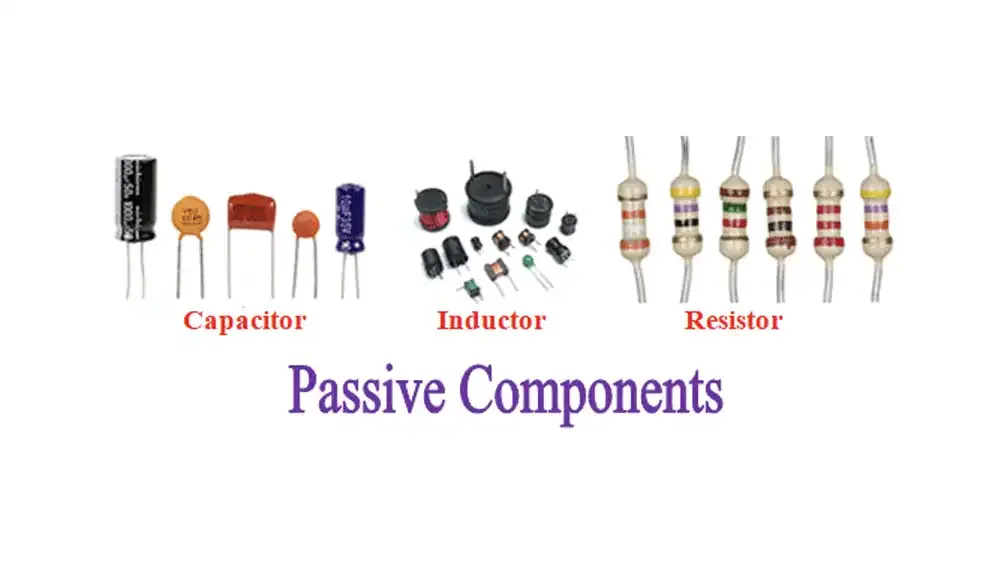
Understanding Through-Hole Components
Through-hole components are electronic parts with leads (metal wires or pins) designed to be inserted into drilled holes on a PCB. These components come in various shapes and sizes, each serving specific functions. Common types include:
- Resistors and Capacitors: Axial or radial lead components used for basic circuit functions like limiting current or storing charge. For example, a 1kΩ resistor might have axial leads for through-hole mounting.
- Diodes and LEDs: Used for directing current flow or providing visual indicators. Their leads are typically long enough to pass through the PCB for secure soldering.
- Transistors: Often used in amplification or switching, transistors like the TO-220 package are commonly mounted via through-hole for heat dissipation.
- Connectors: Components like pin headers or terminal blocks rely on through-hole mounting for a robust connection to external wiring.
- Integrated Circuits (ICs): Dual in-line package (DIP) ICs with through-hole pins are popular in educational projects and older designs due to ease of use.
These components are selected based on the circuit’s needs, including power rating, voltage tolerance (e.g., a capacitor rated for 50V), and physical size. Their leads must align with the PCB’s hole spacing, typically standardized at 0.1 inches (2.54mm) for many designs.
The Through-Hole Assembly Process: Step by Step
The through-hole assembly process involves several key steps to ensure components are securely mounted and electrically connected. Here’s a detailed breakdown:
1. PCB Design and Drilling
The process begins with designing the PCB layout, ensuring holes are placed where component leads will be inserted. These holes are typically drilled with precision to match the lead diameter, often ranging from 0.7mm to 1.2mm, depending on the component. The holes may be plated with copper to enhance conductivity and strength, creating what’s known as plated through-holes (PTH).
2. Component Insertion
Components are inserted into the designated holes, either manually for small runs or using automated insertion machines for larger production. Leads are pushed through from the top side of the PCB, protruding on the bottom side for soldering. Proper alignment is critical to avoid bending leads or damaging the board.
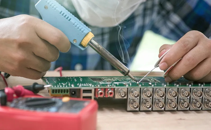
3. Soldering
Soldering secures the component leads to the PCB pads, forming a reliable electrical connection. There are three primary soldering methods used in through-hole assembly, which we’ll explore in detail below: wave soldering, selective soldering, and manual soldering.
4. Inspection and Testing
After soldering, the PCB undergoes visual inspection and testing to ensure all connections are intact and there are no defects like cold solder joints or bridges. Automated optical inspection (AOI) or manual checks with a multimeter can verify continuity and resistance values, such as ensuring a resistor connection measures close to its rated 1kΩ.
5. Trimming Excess Leads
Finally, excess lead length on the underside of the PCB is trimmed using cutters to prevent short circuits and improve the board’s appearance. This step is often done manually or with automated tools in high-volume production.
Soldering Techniques for Through-Hole Assembly
Soldering is the heart of through-hole assembly, and choosing the right technique depends on production volume, component complexity, and precision requirements. Below, we cover the three main methods: wave soldering, selective soldering, and manual soldering techniques.
Wave Soldering for High-Volume Production
Wave soldering is a bulk soldering method ideal for mass production of through-hole PCBs. In this process, the PCB is passed over a wave of molten solder, typically at a temperature of 250–260°C, which coats the exposed leads and pads on the underside of the board. A flux layer is applied beforehand to clean the surfaces and ensure proper adhesion.
Advantages:
- Fast and efficient for large batches, soldering hundreds of connections in seconds.
- Consistent results with minimal human intervention.
Challenges:
- Not suitable for double-sided boards with surface-mount components on the bottom side, as the wave can damage them.
- Requires precise control to avoid solder bridges or insufficient wetting.
Tip: Ensure proper preheating of the PCB (typically to 100–120°C) before wave soldering to prevent thermal shock, which can crack components or warp the board.
Selective Soldering for Precision
Selective soldering is a more targeted approach, often used for mixed-technology boards with both through-hole and surface-mount components. It uses a programmable solder fountain to apply solder only to specific areas, avoiding sensitive components or areas already soldered.
Advantages:
- Highly precise, reducing the risk of damaging nearby components.
- Ideal for complex designs or rework scenarios.
Challenges:
- Slower than wave soldering, making it less cost-effective for high-volume runs.
- Requires skilled programming of the soldering equipment.
Tip: Use selective soldering when working with high-density boards where through-hole components are near heat-sensitive parts, ensuring temperatures remain below critical thresholds like 150°C for certain ICs.
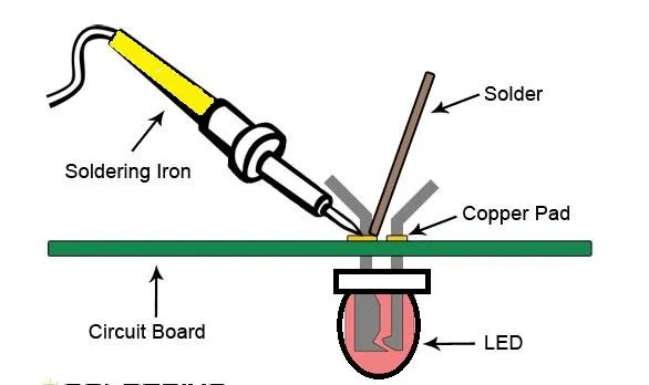
Manual Soldering Techniques for Small Runs and Repairs
Manual soldering is the go-to method for prototypes, small batches, or repairs. It involves using a soldering iron, typically with a tip temperature of 300–350°C, to apply solder to each joint individually. This technique requires skill to achieve clean, reliable connections without damaging the PCB or components.
Key Steps for Manual Soldering:
- Prepare the Iron: Use a clean, tinned tip to ensure efficient heat transfer. A 25W–40W iron is suitable for most through-hole work.
- Apply Flux: Add flux to the joint to remove oxidation and improve solder flow.
- Heat the Joint: Place the iron tip on both the lead and pad for 2–3 seconds to heat them evenly.
- Add Solder: Feed solder wire into the joint, allowing it to melt and form a shiny, conical shape. Avoid excessive solder to prevent bridges.
- Cool and Inspect: Let the joint cool naturally (avoid blowing on it) and check for a smooth, glossy finish.
Advantages:
- Cost-effective for low-volume or one-off projects.
- Offers flexibility for custom or intricate designs.
Challenges:
- Time-consuming for large boards with many components.
- Prone to human error, such as cold joints or overheating (which can lift pads if the iron exceeds 400°C for too long).
Tip: Practice on scrap boards to perfect your manual soldering techniques, ensuring consistent joint quality before working on critical projects.
Suggested Reading: Beginner's Guide: Setting Up Your First Manual Soldering Station for Electronics Projects
Tips for Successful Through-Hole PCB Assembly
To achieve high-quality results in through-hole assembly, consider these practical tips tailored to engineers and hobbyists alike:
- Choose the Right Hole Size: Ensure drilled holes are slightly larger than component leads (e.g., 0.1mm larger) for easy insertion without excessive play, which can lead to weak joints.
- Use Quality Solder and Flux: Opt for lead-free solder with a rosin core for environmental compliance and better wetting. A no-clean flux can reduce post-soldering cleanup.
- Maintain Cleanliness: Keep the PCB and components free of dust or grease before soldering to prevent poor connections. Use isopropyl alcohol (90% or higher) for cleaning if needed.
- Control Soldering Temperature: Avoid overheating components or pads. For sensitive parts like LEDs, keep soldering time under 5 seconds per joint and use a heat sink if necessary.
- Double-Check Polarity: For polarized components like diodes or electrolytic capacitors, verify orientation before soldering to avoid circuit failure.
- Secure Components Before Soldering: Bend leads slightly after insertion or use a temporary adhesive to hold components in place during soldering, especially for larger parts.
Advantages and Limitations of Through-Hole Assembly
Understanding the pros and cons of through-hole assembly helps in making informed decisions for your projects.
Advantages
- Durability: Strong mechanical bonds withstand physical stress and environmental challenges.
- Ease of Repair: Components can be desoldered and replaced without specialized equipment, unlike many SMT parts.
- Better Heat Dissipation: Ideal for high-power components that generate significant heat, such as voltage regulators dissipating 2W or more.
Limitations
- Space Constraints: Takes up more board space, limiting use in compact or portable devices.
- Higher Cost in Mass Production: Drilling holes and manual insertion increase manufacturing time and cost compared to SMT automation.
- Signal Integrity Issues: Longer leads can introduce parasitic inductance, affecting high-frequency performance above 100MHz in some designs.
Conclusion
Through-hole PCB assembly remains a vital technique in electronics manufacturing, offering unmatched reliability for applications where durability and mechanical strength are paramount. Whether you’re using wave soldering for high-volume production, selective soldering for precision on mixed boards, or manual soldering techniques for prototypes, understanding the through-hole assembly process ensures better outcomes. By selecting the right through-hole components and following best practices, you can build robust circuits suited for demanding environments.
At ALLPCB, we’re committed to supporting your PCB assembly needs, from design to production. Whether you’re tackling a high-power industrial project or a small-scale prototype, through-hole assembly could be the key to your success. Explore our services to bring your ideas to life with precision and quality.


