 ALLPCB


In the fast-paced world of electronics manufacturing, ensuring the quality and reliability of printed circuit boards (PCBs) is critical. One of the most effective methods to achieve this is through PCB X-ray inspection. But what exactly is PCB X-ray inspection, and how can it benefit your production process? This comprehensive guide will walk you through the essentials of the PCB X-ray inspection process, the equipment used, associated costs, and available services, helping you make informed decisions for your projects.
Whether you're an engineer, a quality control manager, or a business owner in the electronics industry, understanding how this advanced technology works can save you time, reduce defects, and ensure your products meet the highest standards. Let’s dive into the details of PCB X-ray inspection and explore why it’s a game-changer for modern manufacturing.
What Is PCB X-ray Inspection and Why Does It Matter?
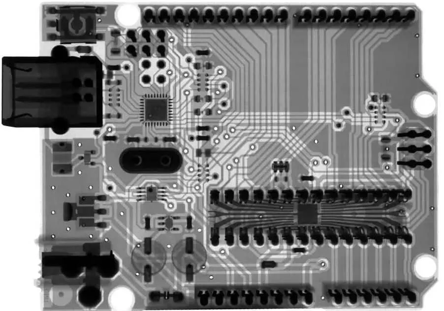
PCB X-ray inspection is a non-destructive testing method used to examine the internal structure of a printed circuit board. Unlike traditional visual inspections, which can only assess surface-level issues, X-ray inspection reveals hidden defects such as soldering flaws, misaligned components, or internal cracks that are invisible to the naked eye. This technology uses X-ray radiation to penetrate the board and create detailed images of its internal layers, helping manufacturers identify problems before they lead to product failures.
The importance of this inspection method cannot be overstated. In industries like aerospace, medical devices, and automotive electronics, even a minor defect in a PCB can result in catastrophic consequences. By incorporating X-ray inspection into the quality control process, manufacturers can ensure reliability, improve yield rates, and maintain customer trust. This guide will break down every aspect of this technology, from the process to the equipment, costs, and service options available.
Understanding the PCB X-ray Inspection Process
The PCB X-ray inspection process is a systematic approach to detecting defects and ensuring the structural integrity of a circuit board. Below, we outline the key steps involved in this method, giving you a clear picture of how it works in a manufacturing setting.
Step 1: Preparation of the PCB for Inspection
Before the X-ray inspection begins, the PCB is prepared and positioned in the inspection machine. This involves securing the board in a way that allows for optimal imaging. Technicians ensure that the board is clean and free from any external contaminants that could interfere with the X-ray results. Proper alignment is crucial to capture accurate images of the specific areas of interest, such as solder joints or multilayer connections.
Step 2: X-ray Imaging and Data Collection
Once the PCB is in place, the X-ray machine emits controlled radiation to penetrate the board. Different materials within the PCB, such as copper traces, solder, and components, absorb varying levels of radiation, creating a contrast in the resulting image. Advanced systems can produce 2D or even 3D images, allowing for a detailed view of internal structures. For instance, a typical X-ray system might operate at a voltage range of 50-160 kV, depending on the thickness and density of the board being inspected.
Step 3: Analysis of X-ray Images
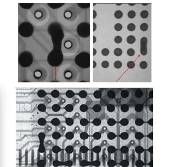
After capturing the images, specialized software processes the data to highlight potential defects. Common issues detected include voids in solder joints (which can weaken connections), misaligned ball grid array (BGA) components, or broken traces in multilayer boards. Engineers analyze these images to determine if the PCB meets the required standards, often referring to industry benchmarks like IPC-A-610 for acceptability criteria.
Step 4: Reporting and Decision-Making
The final step involves generating a detailed report of the findings. This report includes images, defect locations, and recommendations for rework or rejection if necessary. Manufacturers use this information to decide whether a PCB can proceed to the next production stage or if it requires repairs. This step ensures that only high-quality boards reach the end user.
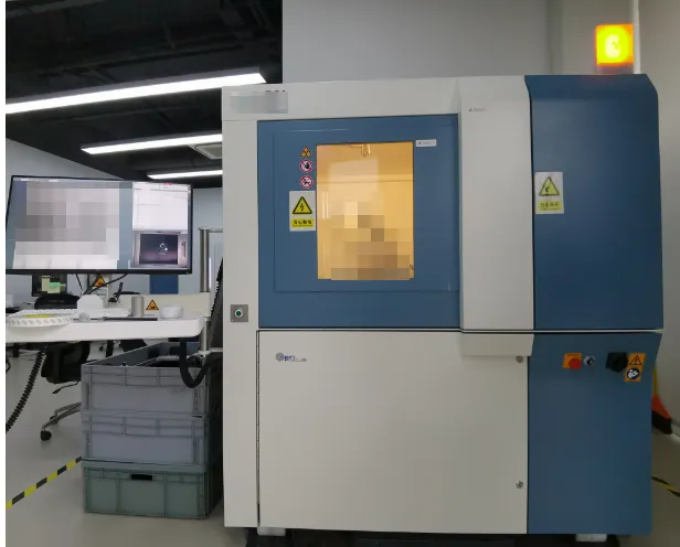
PCB X-ray Inspection Equipment: Tools for Precision
The effectiveness of PCB X-ray inspection largely depends on the quality and capabilities of the equipment used. Modern X-ray systems are designed to handle a wide range of PCB types, from simple single-layer boards to complex multilayer designs. Let’s explore the key types of equipment and their features.
Types of X-ray Inspection Systems
There are primarily two types of X-ray systems used for PCB inspection: 2D and 3D systems. 2D systems are more common and cost-effective, providing a flat image of the board’s internal structure. They are ideal for detecting basic defects like solder joint issues. On the other hand, 3D systems, often referred to as computed tomography (CT) scanners, offer a more comprehensive view by reconstructing a three-dimensional model of the PCB. These are particularly useful for inspecting densely populated boards with hidden components, though they come at a higher cost.
Key Features to Look for in Equipment
When selecting PCB X-ray inspection equipment, consider factors like resolution, magnification, and imaging speed. High-resolution systems can detect defects as small as 1 micrometer, which is critical for microelectronics. Magnification levels of up to 1000x are often necessary to inspect fine-pitch components. Additionally, automated systems with real-time imaging capabilities can significantly reduce inspection time, boosting production efficiency.
Maintenance and Safety Considerations
X-ray equipment requires regular maintenance to ensure consistent performance. This includes calibrating the system to maintain image accuracy and checking for radiation leaks to protect operators. Safety is a top priority, as X-ray machines emit radiation that can be harmful if not properly managed. Most modern systems are equipped with shielding and safety interlocks to minimize exposure risks, adhering to international safety standards.
PCB X-ray Inspection Cost: What to Expect
Understanding the cost of PCB X-ray inspection is essential for budgeting and planning in electronics manufacturing. The expenses associated with this technology vary based on several factors, including the type of equipment, the complexity of the inspection, and whether you opt for in-house inspection or outsourced services.
Factors Influencing Inspection Costs
The cost of PCB X-ray inspection can range widely depending on the scope of the project. For instance, inspecting a simple single-layer board might cost significantly less than a multilayer board with hundreds of components. The price of equipment itself can range from $50,000 for basic 2D systems to over $500,000 for advanced 3D CT scanners. Additionally, operational costs such as technician training, software licensing, and maintenance can add up over time.
In-House vs. Outsourced Inspection
Manufacturers face a choice between investing in their own X-ray inspection setup or outsourcing to specialized service providers. Setting up an in-house system requires a significant upfront investment but offers long-term control and flexibility. For smaller operations, outsourcing may be more cost-effective, with inspection fees typically ranging from $100 to $500 per board, depending on the complexity and volume. Weighing the pros and cons of each option is crucial to determine the best fit for your needs.
Cost-Saving Tips
To manage costs effectively, consider batching inspections to reduce per-unit expenses, especially if outsourcing. Investing in automated systems can also lower labor costs over time by minimizing manual analysis. Additionally, regular maintenance of equipment can prevent costly downtime and repairs, ensuring a better return on investment.
PCB X-ray Inspection Services: Finding the Right Partner
For many manufacturers, especially small to medium-sized enterprises, outsourcing PCB X-ray inspection services is a practical solution. These services provide access to state-of-the-art equipment and expert technicians without the burden of owning and maintaining costly systems. Here’s what you need to know about choosing the right service provider.
Benefits of Professional Inspection Services
Outsourcing to a professional service offers several advantages, including access to advanced technology and expertise. Service providers often employ highly trained engineers who can interpret complex X-ray images and provide detailed reports. This can be particularly valuable for industries with strict compliance requirements, as these providers are well-versed in standards like ISO 9001 and IPC guidelines.
How to Choose a Service Provider
When selecting a PCB X-ray inspection service, look for providers with a proven track record in your industry. Check for certifications and ask about their equipment capabilities—do they offer both 2D and 3D imaging? Turnaround time is another critical factor; ensure the provider can meet your production deadlines. Finally, consider their reporting process—clear, actionable reports with detailed images are essential for effective decision-making.
Industries Served by Inspection Services
PCB X-ray inspection services cater to a wide range of industries, from consumer electronics to aerospace. For example, in the medical device sector, X-ray inspection ensures that PCBs in life-saving equipment like pacemakers are defect-free. In automotive manufacturing, it verifies the reliability of electronic control units that manage critical systems. Regardless of your field, there’s likely a service tailored to your specific quality needs.
Benefits of PCB X-ray Inspection for Quality Assurance
Implementing PCB X-ray inspection as part of your quality assurance strategy offers numerous benefits that directly impact your bottom line and reputation. Here are some of the key advantages:
- Early Defect Detection: Identifying issues like solder voids or misalignments early in the production process prevents costly rework and product recalls.
- Non-Destructive Testing: Unlike other methods that may damage the board, X-ray inspection preserves the integrity of the PCB while providing detailed insights.
- Improved Product Reliability: By ensuring that internal connections are flawless, X-ray inspection enhances the overall performance and lifespan of electronic devices.
- Compliance with Standards: This method helps manufacturers meet stringent industry standards, which is crucial for regulated sectors like medical and aerospace.
With defect rates in electronics manufacturing sometimes reaching as high as 5-10% without proper inspection, integrating X-ray technology can reduce this figure significantly, often to below 1%, depending on the complexity of the design.
Challenges and Limitations of PCB X-ray Inspection
While PCB X-ray inspection is a powerful tool, it’s not without its challenges. Understanding these limitations can help you set realistic expectations and plan accordingly.
High Initial Investment
As mentioned earlier, the cost of purchasing and maintaining X-ray equipment can be prohibitive for smaller manufacturers. Even with outsourcing, fees for high-volume or complex inspections can add up quickly.
Technical Expertise Required
Interpreting X-ray images requires specialized training. Without skilled technicians, there’s a risk of misdiagnosis, which could lead to overlooking critical defects or unnecessary rework.
Time Constraints
While automated systems have improved inspection speeds, analyzing detailed 3D images can still be time-consuming, especially for intricate designs. Balancing speed with accuracy is a constant challenge in high-throughput environments.
Despite these hurdles, the benefits of X-ray inspection often outweigh the drawbacks, especially when quality and reliability are non-negotiable.
Future Trends in PCB X-ray Inspection
The field of PCB X-ray inspection is evolving rapidly, driven by advancements in technology and the increasing complexity of electronic devices. Here are some trends to watch for in the coming years:
- Integration with AI: Artificial intelligence is being incorporated into X-ray systems to automate defect detection and reduce human error. AI algorithms can analyze images faster and with greater accuracy, identifying patterns that might be missed by the human eye.
- Miniaturization of Equipment: As PCBs become smaller and more compact, X-ray systems are also shrinking in size while maintaining high resolution, making them more accessible for smaller manufacturers.
- Enhanced 3D Imaging: Improvements in 3D CT scanning technology are providing even clearer images of multilayer boards, allowing for more precise inspections of densely packed components.
These innovations promise to make PCB X-ray inspection more efficient and cost-effective, further solidifying its role in quality control.
Conclusion: Elevate Your PCB Quality with X-ray Inspection
PCB X-ray inspection is an indispensable tool for ensuring the quality and reliability of printed circuit boards in today’s competitive electronics market. From understanding the detailed PCB X-ray inspection process to investing in the right equipment, managing costs, and choosing reliable services, this guide has covered everything you need to know to make informed decisions. By leveraging this advanced technology, you can detect hidden defects, improve product performance, and maintain compliance with industry standards.
At ALLPCB, we’re committed to supporting your manufacturing journey with cutting-edge solutions and expert guidance. Whether you’re looking to integrate X-ray inspection into your process or seeking trusted partners for outsourced services, we’re here to help you achieve excellence in every project. Embrace the power of PCB X-ray inspection and take your quality assurance to the next level.


