 ALLPCB


Reflow soldering is a cornerstone of modern PCB assembly, but how does it affect Hi-Pot testing performance for assembled printed circuit boards? In short, reflow soldering can influence Hi-Pot testing outcomes by impacting solder joint integrity, introducing potential defects like voids or cracks, and affecting dielectric strength between conductive paths. Factors such as thermal stress during reflow, solder paste quality, and PCB design play a critical role in determining whether a board passes or fails a Hi-Pot test after reflow. In this blog, we’ll dive deep into the relationship between reflow soldering and Hi-Pot testing, exploring how to ensure reliable results and maintain high-quality PCB assemblies. Let’s break down the key aspects of “Reflow Hi-Pot impact,” “soldering and testing,” and “test after reflow” to provide actionable insights for engineers and manufacturers.
What is Reflow Soldering and Why Does It Matter?
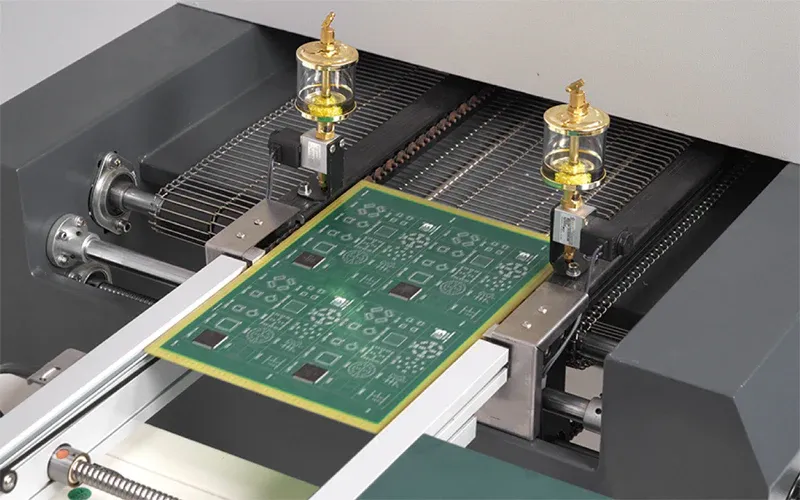
Reflow soldering is a widely used technique in surface mount technology (SMT) for attaching components to printed circuit boards (PCBs). During this process, solder paste—a mix of tiny solder particles and flux—is applied to the board’s pads. Components are then placed on the paste, and the entire assembly is heated in a controlled manner inside a reflow oven. The heat melts the solder, creating permanent joints as it cools and solidifies.
This method is essential for high-volume production due to its efficiency and ability to handle complex designs with thousands of tiny components. However, the thermal cycles involved—often reaching temperatures of 220°C to 260°C—can introduce stresses on the PCB materials and components. These stresses, if not managed properly, may lead to issues like solder joint cracking, delamination of board layers, or even microscopic voids in the solder. Such defects are critical when it comes to “solder joint integrity” and can directly influence the performance during electrical tests like Hi-Pot testing.
Understanding Hi-Pot Testing in PCB Assembly
Hi-Pot testing, short for High Potential testing, is a crucial quality control step in PCB manufacturing. It checks the dielectric strength of a board by applying a high voltage—often between 500V and 3000V, depending on the application—between different conductive paths or between conductors and ground. The goal is to ensure that the insulation between these paths can withstand the voltage without breaking down, which could lead to short circuits or safety hazards.
For assembled PCBs, Hi-Pot testing is typically performed after soldering to verify that the board can handle real-world electrical stresses. A failure in this test might indicate issues like insufficient spacing between traces, contamination, or defects introduced during assembly processes like reflow soldering. This is why understanding the “PCB test influence” of soldering processes is vital for manufacturers aiming for reliability and safety in their products.
How Reflow Soldering Impacts Hi-Pot Testing Performance
The reflow soldering process can affect Hi-Pot testing outcomes in several ways. Below, we explore the key factors contributing to this “Reflow Hi-Pot impact” and how they relate to “test after reflow” scenarios.
1. Thermal Stress and Material Degradation
During reflow soldering, PCBs are exposed to high temperatures for a specific duration, typically following a profile with preheat, soak, reflow, and cooling stages. If the temperature ramps up too quickly or exceeds the tolerance of the PCB substrate (like FR-4, which can degrade above 260°C), it can cause warping or delamination. These physical changes might reduce the dielectric strength of the board, leading to Hi-Pot test failures even if the solder joints themselves are intact.
For instance, a study on PCB materials showed that prolonged exposure to temperatures above 250°C can reduce the dielectric breakdown voltage of FR-4 by up to 15%. This degradation directly impacts the board’s ability to pass high-voltage tests, highlighting the need for precise control over reflow profiles.
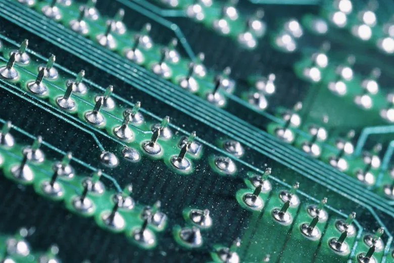
2. Solder Joint Integrity and Defects
“Solder joint integrity” is a critical factor in PCB performance. Poorly formed joints—due to issues like insufficient solder paste, incorrect reflow temperatures, or contamination—can create voids or cracks. These defects act as weak points where electrical arcing can occur during Hi-Pot testing, especially under high voltages. For example, a solder joint with a void percentage above 25% is significantly more likely to fail under a 1000V Hi-Pot test compared to a joint with minimal voids.
Moreover, defects like solder balls or bridging (where solder connects adjacent pads unintentionally) can reduce the effective spacing between conductive paths. This reduction increases the risk of dielectric breakdown during testing, making “soldering and testing” a paired concern for quality assurance.
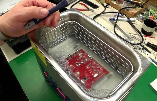
3. Flux Residue and Contamination
Solder paste contains flux to clean surfaces and promote wetting during reflow. However, if flux residues are not properly cleaned after soldering, they can attract moisture or dust over time. This contamination can create conductive paths on the board’s surface, lowering its insulation resistance and causing Hi-Pot test failures. For instance, boards tested at 2000V often fail if surface contamination reduces insulation resistance below 100 MΩ.
Choosing the right type of flux (like no-clean or water-soluble) and ensuring thorough post-reflow cleaning are essential steps to mitigate this risk during “test after reflow” stages.
4. Component and Layout Considerations
The design of the PCB itself, including component placement and trace spacing, interacts with the reflow process to influence Hi-Pot results. Components with tight spacing or high-voltage requirements are more susceptible to failure if reflow soldering introduces even minor misalignments or defects. Additionally, thermal expansion during reflow can shift components slightly, reducing effective clearance distances and impacting test performance.
For high-voltage applications, engineers often design boards with clearances of at least 0.1mm per 100V of test voltage to account for potential shifts during soldering. This proactive approach helps ensure reliability during Hi-Pot testing.
Best Practices to Minimize Reflow Soldering Impact on Hi-Pot Testing
To achieve consistent Hi-Pot test results after reflow soldering, manufacturers must adopt strategies that address the challenges outlined above. Here are practical steps to improve outcomes for “soldering and testing” processes.
1. Optimize Reflow Temperature Profiles
A well-designed reflow profile is key to preventing thermal stress and ensuring proper solder joint formation. The profile should include a gradual preheat stage (1.5-2.5°C per second) to minimize thermal shock, a soak zone to activate flux, and a peak reflow temperature that matches the solder paste’s melting point (typically 220-245°C for lead-free solder). Cooling should also be controlled to avoid rapid contraction, which can crack joints.
Monitoring the profile with thermocouples attached to the PCB ensures accuracy. Deviations as small as 5°C from the ideal peak temperature can increase defect rates by up to 10%, directly affecting Hi-Pot performance.
2. Use High-Quality Solder Paste
The choice of solder paste impacts joint quality significantly. Opt for pastes with consistent particle size distribution and appropriate flux activity to reduce voids and ensure uniform melting. For example, Type 3 or Type 4 solder pastes (with particle sizes of 25-45 μm or 20-38 μm, respectively) are often recommended for fine-pitch components to minimize defects during reflow.
3. Implement Thorough Cleaning Processes
Post-reflow cleaning removes flux residues and other contaminants that could compromise insulation resistance. Aqueous cleaning systems or solvent-based solutions can achieve surface cleanliness levels that maintain insulation resistance above 500 MΩ, a common threshold for passing Hi-Pot tests at 1000V or higher.
4. Conduct Pre-Test Inspections
Before Hi-Pot testing, perform visual and automated optical inspections (AOI) to detect solder defects like bridging or insufficient joints. X-ray inspection can also identify hidden voids in solder joints under components like BGAs. Addressing these issues before testing reduces the likelihood of failures and costly rework.
5. Design for Testability
Incorporate Hi-Pot testing requirements into the PCB design phase. Ensure adequate spacing between high-voltage traces (e.g., 0.5mm for 500V applications) and use conformal coatings if needed to enhance insulation. These design choices help mitigate the “PCB test influence” of reflow soldering defects.
Common Challenges and Solutions in “Test After Reflow”
Even with best practices, challenges can arise during Hi-Pot testing post-reflow. Here are some common issues and how to address them:
- Issue: Frequent Hi-Pot Failures Due to Arcing
Solution: Inspect for solder bridges or insufficient clearance. Increase spacing in future designs and refine reflow profiles to prevent excess solder flow. - Issue: Inconsistent Test Results
Solution: Standardize cleaning processes and ensure test equipment is calibrated to apply consistent voltage levels, such as 1000V ±5%. - Issue: Component Damage During Testing
Solution: Verify that components are rated for the test voltage and protect sensitive parts with temporary shielding if necessary.
The Importance of Collaboration in PCB Manufacturing
Achieving reliable Hi-Pot test results after reflow soldering requires collaboration between design engineers, assembly teams, and quality control specialists. Designers must account for thermal and electrical stresses, while assembly teams ensure precise soldering conditions. Quality control validates the final product through rigorous testing, closing the loop on “soldering and testing” workflows.
By fostering communication across these teams, manufacturers can identify potential issues early—whether it’s a design flaw affecting clearance or a reflow parameter causing joint defects—and implement corrective actions before testing begins.
Conclusion: Balancing Reflow Soldering and Hi-Pot Testing for Success
Reflow soldering is a powerful process for assembling PCBs, but its impact on Hi-Pot testing performance cannot be overlooked. Thermal stress, solder joint defects, contamination, and design factors all play a role in determining whether a board passes a high-voltage test after reflow. By optimizing reflow profiles, using quality materials, cleaning thoroughly, and designing with testing in mind, manufacturers can minimize the “Reflow Hi-Pot impact” and ensure reliable, high-performing PCBs.
Understanding the connection between “soldering and testing” is essential for engineers and manufacturers aiming to deliver safe and durable electronic products. With the right practices in place, the challenges of “test after reflow” can be managed effectively, ensuring “solder joint integrity” and reducing the “PCB test influence” of soldering defects. At ALLPCB, we’re committed to supporting your journey toward flawless PCB assembly and testing—every step of the way.


