 ALLPCB


In the world of high-speed electronics, ensuring signal integrity is critical for reliable performance. One often overlooked factor in this process is PCB drilling. How does PCB drilling affect signal integrity? Simply put, the precision and design of drilled holes, especially vias, directly influence signal reflection, impedance control, and overall performance in high-frequency PCB design. Poor drilling practices can lead to signal losses, delays, and interference, while optimized techniques can enhance performance.
In this detailed guide, we’ll explore the relationship between PCB drilling and signal integrity, focusing on via design, signal reflection, impedance control, and PCB drilling best practices. Whether you’re designing for high-frequency applications or standard circuits, understanding these concepts will help you minimize losses and optimize performance.
Why PCB Drilling Matters for Signal Integrity
Printed Circuit Boards (PCBs) are the backbone of modern electronics, connecting components and enabling signal transmission. Drilling is a fundamental step in PCB manufacturing, creating holes for vias, through-holes, and mounting components. However, drilling isn’t just about making holes—it’s about precision. In high-frequency PCB design, even small imperfections in drilled holes can disrupt signal paths, causing reflections, delays, or noise.
Signal integrity refers to the quality of an electrical signal as it travels through a PCB. When signals encounter issues like impedance mismatches or physical obstructions, their integrity degrades, leading to data errors or system failures. Since vias (drilled holes that connect different layers of a PCB) are critical signal pathways, their design and drilling quality play a huge role in maintaining clean signal transmission.
The Role of Via Design in Signal Integrity
Vias are small drilled holes that allow signals to pass between layers of a multilayer PCB. While they are essential for compact designs, vias can introduce signal integrity issues if not designed or drilled properly. Let’s break down how via design impacts performance in high-frequency PCB design.
Via Types and Their Effects
There are several types of vias, each with unique characteristics:
- Through-Hole Vias: These pass through all layers of the PCB. While they are simple to manufacture, they can create long signal paths, increasing the risk of signal reflection and delay in high-frequency designs.
- Blind Vias: These connect an outer layer to an inner layer without passing through the entire board. They reduce signal path length but require precise drilling to avoid misalignment.
- Buried Vias: Located entirely within inner layers, buried vias are ideal for high-density designs but are more challenging to drill accurately.
- Microvias: Tiny vias used in high-density interconnect (HDI) boards. They minimize signal path length but demand extremely precise drilling techniques.
In high-frequency designs operating above 1 GHz, shorter vias like blind or microvias are preferred because they reduce inductance and signal delay. For example, a through-hole via might introduce a delay of 50-100 picoseconds, while a microvia can cut this down significantly.
Via Placement and Signal Reflection
Signal reflection occurs when a signal encounters an impedance mismatch, sending part of the signal back toward the source. Vias are common culprits for reflections because they can act as discontinuities in the signal path. Poorly placed or oversized vias can worsen this effect.
To minimize reflections, vias should be placed close to the signal source or termination point. Additionally, maintaining consistent via pad sizes and avoiding unnecessary vias in critical signal paths can help. For instance, in a 5 GHz signal path, a via with a pad diameter of 0.5 mm might cause a noticeable reflection, while reducing it to 0.3 mm can improve performance.
Impedance Control and PCB Drilling
Impedance control is a cornerstone of signal integrity, especially in high-frequency PCB design. Impedance refers to the resistance a signal faces as it travels through a trace or via. Any mismatch in impedance can cause signal reflections and losses.
How Drilling Affects Impedance
The size, shape, and finish of a drilled via directly impact its impedance. For example, a via with a rough inner wall (due to poor drilling quality) can increase parasitic capacitance, altering the impedance. Similarly, an oversized via hole can disrupt the surrounding dielectric material, causing an impedance mismatch.
In a typical high-speed design, traces are designed for a specific impedance, often 50 ohms for RF applications. If a via’s impedance deviates by even 5-10 ohms due to drilling inaccuracies, it can cause significant signal distortion. Advanced drilling techniques, such as laser drilling for microvias, ensure smoother walls and tighter tolerances, helping maintain consistent impedance.
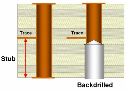
Back-Drilling for Impedance Optimization
Back-drilling is a specialized technique used to remove unused portions of through-hole vias. In high-frequency designs, the unused stub of a via can act as a resonant structure, causing reflections. By drilling out this stub, back-drilling reduces impedance mismatches and improves signal integrity. For signals operating at 10 GHz, back-drilling can reduce stub-related losses by up to 20%.
PCB Drilling Best Practices for Signal Integrity
To achieve optimal signal integrity, following PCB drilling best practices is essential. These guidelines focus on precision, material considerations, and design optimization.
1. Choose the Right Drilling Method
Mechanical drilling is common for standard PCBs, but it can cause burrs or rough edges that affect signal paths. For high-frequency designs, laser drilling is preferred because it offers higher precision and smoother hole walls. Laser-drilled microvias, for instance, can achieve diameters as small as 0.1 mm, reducing parasitic effects.
2. Optimize Via Size and Aspect Ratio
The aspect ratio of a via (the ratio of hole depth to diameter) should be kept low to ensure plating uniformity and signal quality. A ratio of 8:1 or lower is ideal for most designs. For a 1.6 mm thick PCB, this means keeping via diameters at 0.2 mm or larger. Smaller vias may look appealing for space-saving, but they can be harder to drill accurately and may lead to manufacturing defects.
3. Use High-Quality Materials
The PCB material around drilled holes affects signal integrity. Low-loss dielectrics with a dielectric constant (Dk) of 3.0-3.5 are ideal for high-frequency applications because they minimize signal attenuation. Drilling through such materials requires care to avoid cracking or delamination, which can alter impedance.
4. Minimize Drill Wander and Misalignment
Drill wander—when the drill bit deviates from its intended path—can misalign vias, leading to signal crosstalk or shorts. Modern CNC drilling machines with precision controls can keep wander below 0.05 mm, ensuring vias align perfectly with design specifications.
5. Inspect and Test After Drilling
Post-drilling inspection using X-ray or automated optical inspection (AOI) can detect misaligned or poorly drilled vias before they cause issues. Testing for impedance and signal reflection after drilling also helps identify potential problems early in the manufacturing process.
Challenges in High-Frequency PCB Design
High-frequency PCB design amplifies the challenges of maintaining signal integrity. Signals operating at frequencies above 1 GHz are more sensitive to small imperfections in drilling and via design. Here are some specific issues and solutions:
Signal Attenuation
At high frequencies, signals lose strength as they travel through vias due to dielectric losses and skin effect. Using smaller vias and low-loss materials can reduce attenuation. For example, a signal at 5 GHz might lose 0.5 dB per inch on a standard FR-4 material, but switching to a low-loss material can cut this loss in half.
Crosstalk
Crosstalk occurs when signals in nearby vias or traces interfere with each other. Proper spacing of vias during drilling and the use of ground planes can minimize this. A general rule is to keep high-speed vias at least 3 times the via diameter apart to avoid coupling effects.
Thermal and Mechanical Stress
Drilling generates heat and mechanical stress, which can damage delicate PCB materials or cause micro-cracks near vias. Using controlled drilling speeds and cooling techniques can prevent these issues, ensuring long-term reliability.
Advanced Techniques for Optimizing Performance
Beyond basic drilling best practices, advanced techniques can further enhance signal integrity in demanding applications.
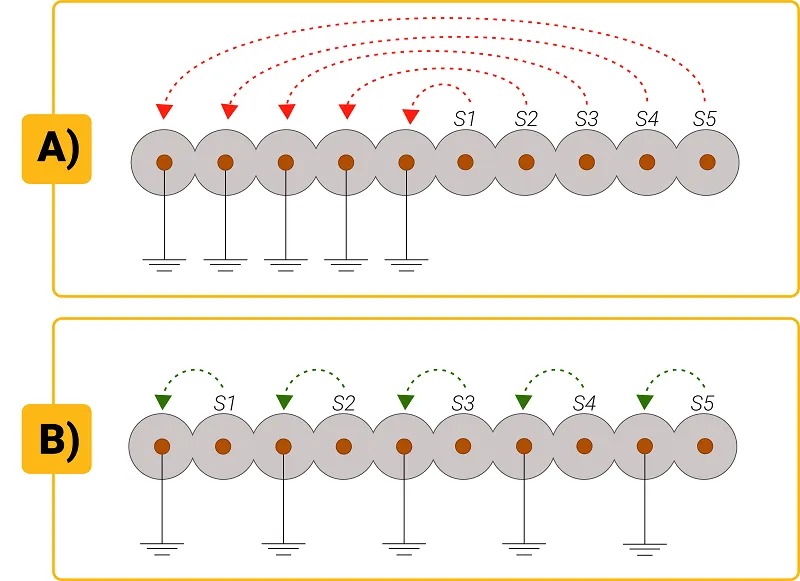
Via Stitching
Via stitching involves placing multiple ground vias around high-speed signal vias to create a low-impedance return path. This technique reduces electromagnetic interference (EMI) and improves signal quality. For a 10 GHz design, via stitching can lower noise levels by up to 15%.
Controlled Depth Drilling
For blind and buried vias, controlled depth drilling ensures the hole reaches the exact layer without overshooting. This precision prevents unnecessary signal stubs and maintains impedance consistency.
Simulation and Modeling
Before drilling, use simulation tools to model signal behavior through vias. These tools can predict impedance mismatches, reflections, and crosstalk, allowing you to adjust via design and placement. For instance, a simulation might show that reducing via pad size from 0.6 mm to 0.4 mm cuts reflection by 10% at 3 GHz.
Conclusion: Balancing Precision and Performance
PCB drilling plays a pivotal role in signal integrity, especially in high-frequency PCB design. From via design to impedance control, every aspect of drilling must be carefully managed to minimize signal reflection and losses. By following PCB drilling best practices—such as using precise drilling methods, optimizing via size, and leveraging advanced techniques like back-drilling and via stitching—you can significantly enhance performance.
Whether you’re working on a simple circuit or a complex high-speed system, paying attention to the details of drilling and via design will ensure your PCB operates reliably. With the right approach, you can achieve clean signal transmission and build electronics that meet the demands of modern technology.


