 ALLPCB


In the fast-evolving world of electronics, Printed Circuit Board (PCB) manufacturing is undergoing a significant transformation. At the heart of this change is the integration of Artificial Intelligence (AI) and Machine Learning (ML) into imaging processes. These technologies are revolutionizing how PCBs are designed, inspected, and manufactured, ensuring higher quality, faster production, and reduced costs. If you're wondering how AI in PCB imaging or machine learning PCB defect detection can enhance manufacturing, the answer lies in automation, precision, and data-driven insights. This blog dives deep into the role of these cutting-edge technologies, exploring automated PCB inspection, deep learning PCB analysis, and the rise of smart PCB manufacturing.
Why AI and Machine Learning Matter in PCB Manufacturing
PCB manufacturing is a complex process that demands precision at every stage, from design to final inspection. Traditional methods often rely on manual checks or basic automated systems, which can be slow and prone to errors. AI and ML bring a new level of intelligence to the table by analyzing vast amounts of data, identifying patterns, and making decisions in real-time. In imaging processes, these technologies help detect defects, optimize designs, and streamline workflows.
For instance, AI in PCB imaging allows systems to process high-resolution images of boards to spot tiny flaws that might escape human eyes. Machine learning algorithms can be trained on thousands of images to recognize specific defect types, such as cracks or misaligned components, with over 95% accuracy in some advanced systems. This not only improves quality control but also cuts down inspection time significantly.
The Role of AI in PCB Imaging
Imaging is a critical part of PCB manufacturing, used for both design verification and quality inspection. AI in PCB imaging leverages advanced algorithms to process and interpret visual data from cameras and scanners. Unlike traditional imaging systems that follow pre-set rules, AI adapts and learns from each image it processes, improving its accuracy over time.
One key application is in the analysis of X-ray images for multilayer PCBs. These boards often have internal layers that are invisible to the naked eye, making defect detection challenging. AI systems can analyze X-ray scans to identify issues like voids in solder joints or misaligned vias with precision. Studies suggest that AI-powered imaging can reduce false positives in defect detection by up to 30% compared to older methods.
Additionally, AI helps in real-time monitoring during the manufacturing process. Cameras equipped with AI can instantly flag issues on the production line, such as incorrect component placement, allowing for immediate corrections. This capability minimizes waste and ensures that only high-quality boards move forward in the production cycle.
Machine Learning PCB Defect Detection: A Game Changer
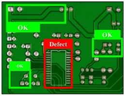
Defect detection is one of the most time-consuming and error-prone aspects of PCB manufacturing. Machine learning PCB defect detection systems are changing the game by automating and refining this process. These systems are trained on datasets containing thousands of images of both defective and flawless PCBs, enabling them to classify defects with remarkable accuracy.
For example, a common defect like a short circuit caused by excess solder can be identified by ML models through pattern recognition. These models analyze features such as solder thickness and spacing, comparing them against ideal parameters. Some advanced ML systems achieve detection rates as high as 98% for surface defects, far surpassing manual inspection capabilities.
Moreover, machine learning can categorize defects into specific types—such as scratches, missing components, or soldering errors—allowing manufacturers to address root causes. By integrating ML into defect detection, production lines can achieve higher throughput while maintaining strict quality standards.
Automated PCB Inspection: Speed and Precision Combined
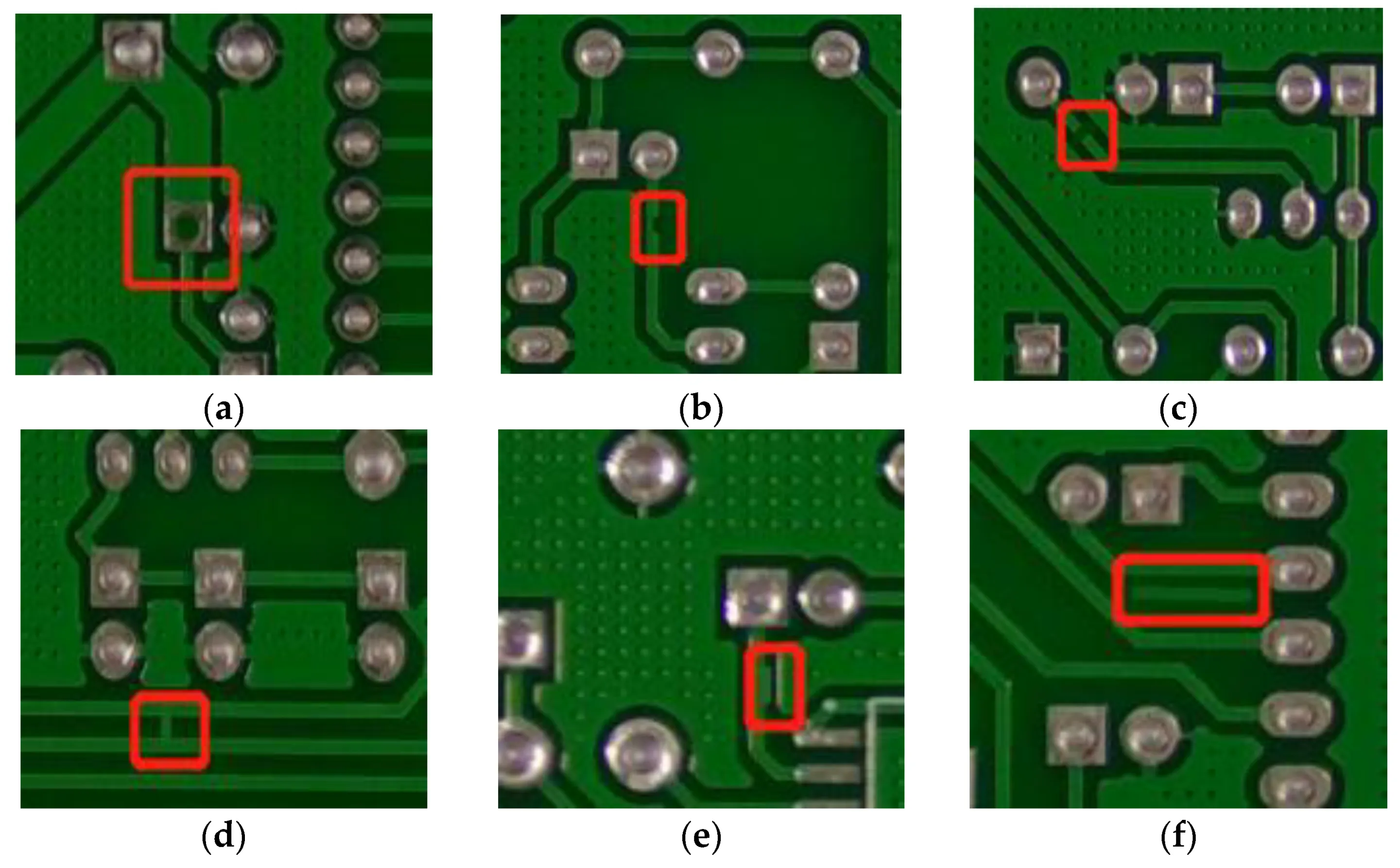
Automated PCB inspection powered by AI and ML is becoming the industry standard for manufacturers aiming to scale production without compromising quality. Traditional inspection methods often involve human operators using microscopes or basic automated optical inspection (AOI) systems. While effective to an extent, these methods struggle with the increasing complexity of modern PCBs, which may feature components as small as 0.4mm in pitch.
AI-driven automated inspection systems use high-speed cameras and advanced algorithms to scan boards in seconds. These systems can detect defects at a resolution of up to 5 micrometers, ensuring even the smallest issues are caught. For instance, in high-density interconnect (HDI) PCBs, automated inspection can identify trace width variations that deviate by just 10 micrometers from the design specs, something nearly impossible for manual checks.
The speed of automated PCB inspection is equally impressive. A typical AI-powered AOI system can inspect hundreds of boards per hour, compared to a human inspector who might manage only a fraction of that number. This efficiency translates to significant cost savings and faster time-to-market for electronic products.
Deep Learning PCB Analysis: Going Beyond Surface-Level Insights
While machine learning excels at identifying known defect patterns, deep learning PCB analysis takes it a step further by uncovering complex, non-linear relationships in data. Deep learning, a subset of ML, uses neural networks with multiple layers to process vast datasets, making it ideal for analyzing intricate PCB designs.
In imaging processes, deep learning models can interpret 3D scans of PCBs to assess internal structures. For example, in a multilayer board with 12 layers, deep learning can detect misalignments between layers that could lead to signal integrity issues, such as impedance mismatches at high frequencies (e.g., above 1 GHz). By identifying these problems early, manufacturers can avoid costly rework or product failures in the field.
Deep learning also enables predictive maintenance for imaging equipment. By analyzing historical data from cameras and scanners, these models can predict when a device might fail or require calibration, ensuring uninterrupted production. Some systems report a 20% reduction in downtime after implementing deep learning-based maintenance schedules.
Smart PCB Manufacturing: The Bigger Picture
The integration of AI and ML into imaging processes is a cornerstone of smart PCB manufacturing. This approach involves creating interconnected, data-driven systems that optimize every stage of production. Smart manufacturing goes beyond inspection—it encompasses design optimization, process control, and supply chain management, all powered by intelligent technologies.
In imaging, smart PCB manufacturing means using AI to not only detect defects but also suggest corrective actions. For instance, if an AI system identifies recurring soldering defects, it can recommend adjustments to the reflow oven temperature or solder paste volume. These insights, derived from real-time data, help manufacturers achieve a defect rate as low as 0.1% in some high-volume production lines.
Furthermore, smart manufacturing enables traceability. AI systems can log every inspection result, linking defects to specific batches or production conditions. This data is invaluable for continuous improvement, allowing manufacturers to refine processes and prevent future issues. As a result, smart PCB manufacturing is paving the way for Industry 4.0, where automation and intelligence drive innovation.
Benefits of AI and ML in PCB Imaging Processes
The adoption of AI and ML in PCB imaging processes offers several tangible benefits:
- Improved Accuracy: AI systems achieve detection accuracies above 95%, reducing the risk of defective boards reaching customers.
- Faster Production: Automated inspection cuts down cycle times, enabling manufacturers to process thousands of boards daily.
- Cost Efficiency: By minimizing rework and scrap, AI and ML reduce production costs by up to 25% in some cases.
- Scalability: These technologies can handle increasing design complexity, supporting the trend toward miniaturization and HDI boards.
- Data Insights: ML models provide actionable insights, helping manufacturers optimize processes and improve yield rates.
Challenges and Future Outlook
Despite the advantages, integrating AI and ML into PCB imaging processes comes with challenges. One major hurdle is the initial investment in hardware and software, which can be significant for small-scale manufacturers. Additionally, training ML models requires large, high-quality datasets, which may not always be available.
Another concern is the need for skilled personnel to manage and maintain AI systems. While the technology automates many tasks, human oversight is still essential to interpret results and make strategic decisions. Overcoming these barriers will require collaboration between technology providers and manufacturers to develop cost-effective, user-friendly solutions.
Looking ahead, the future of smart PCB manufacturing is bright. As AI algorithms become more sophisticated, we can expect even greater precision in defect detection and process optimization. Emerging technologies like edge computing could bring AI processing closer to the production line, reducing latency and enhancing real-time decision-making. By 2030, industry experts predict that over 70% of PCB manufacturers will adopt AI-driven imaging systems as a standard practice.
Conclusion
The future of PCB manufacturing lies in the seamless integration of AI and Machine Learning into imaging processes. From AI in PCB imaging to machine learning PCB defect detection, these technologies are transforming how boards are designed, inspected, and produced. Automated PCB inspection and deep learning PCB analysis are driving unprecedented levels of precision and efficiency, while smart PCB manufacturing is setting the stage for a fully connected, data-driven industry.
For manufacturers, embracing these advancements is no longer optional—it's a necessity to stay competitive in a rapidly changing market. By leveraging AI and ML, companies can achieve higher quality, lower costs, and faster production cycles, ultimately delivering better products to their customers. As this technology continues to evolve, the possibilities for innovation in PCB manufacturing are limitless.


