 ALLPCB


The multilayer printed circuit board (PCB) lamination process is a cornerstone of modern electronics manufacturing, enabling the creation of compact, high-performance devices like smartphones, medical equipment, and aerospace systems. Optimizing this process is critical to achieving reliable, high-quality PCBs that meet stringent performance requirements. In this blog, we explore the multilayer PCB lamination process, key optimization strategies, and practical tips to ensure superior outcomes for engineers and manufacturers.
Understanding the Multilayer PCB Lamination Process
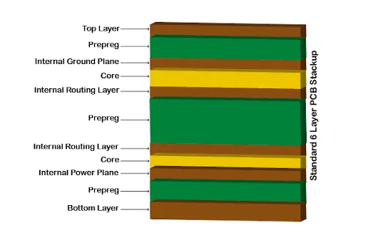
Multilayer PCBs consist of three or more conductive copper layers separated by insulating materials, such as prepreg and core laminates. The lamination process bonds these layers into a single, cohesive board using heat, pressure, and precise alignment. This process is complex, as it must ensure electrical connectivity, structural integrity, and minimal defects like warpage or delamination.
The typical lamination process involves several steps:
1. Stack-Up Preparation: Inner layers (etched with circuit patterns) are stacked with prepreg (resin-impregnated fiberglass) and copper foil in a specific order.
2. Alignment: Layers are aligned using positioning holes or rivets to prevent misalignment.
3. Lamination: The stack is placed in a hydraulic press, where high temperature (around 180-200°C) and pressure (up to 500 psi) are applied to melt the prepreg resin, bonding the layers.
4. Cooling and Inspection: The laminated board is cooled and inspected for defects like layer deviation or voids.
Why Optimization Matters
Optimizing the lamination process directly impacts PCB performance, reliability, and cost. For example, poor lamination can lead to issues like:
- Delamination: Separation of layers due to inadequate bonding, reducing board durability.
- Warpage: Uneven stress causing board bending, which affects component placement.
- Impedance Mismatches: Inconsistent dielectric properties leading to signal integrity issues, critical in high-frequency applications (e.g., 5G devices with impedance values of 50 ± 5 ohms).
By refining the process, manufacturers can achieve tighter tolerances, reduce defects, and improve yield rates, ultimately lowering production costs and ensuring boards meet industry standards like IPC-6012.
Key Strategies for Lamination Process Optimization
1. Material Selection and Compatibility
Choosing the right materials is foundational to successful lamination. The primary materials—prepreg, core, and copper foil—must be compatible in terms of thermal, electrical, and mechanical properties.
- Prepreg: Select prepreg with appropriate resin content (typically 40-60%) to ensure proper flow and bonding. For high-frequency applications, low-loss materials like Rogers 4350B (dielectric constant ~3.48) are preferred.
- Core: Use FR-4 cores for standard applications or ceramic-based cores for high-performance boards (e.g., Alumina with thermal conductivity ~30 W/m·K).
- Copper Foil: Ensure uniform thickness (e.g., 1 oz or 35 µm) to prevent impedance variations.
Compatibility is critical to avoid issues like coefficient of thermal expansion (CTE) mismatches, which can cause warpage. For instance, a CTE mismatch of >10 ppm/°C between layers can lead to significant stress during thermal cycling.
2. Precise Stack-Up Design
A symmetrical stack-up design minimizes warpage and ensures uniform pressure distribution during lamination. Key considerations include:
- Layer Symmetry: Arrange layers so that copper density and dielectric thickness are balanced on both sides of the board's centerline.
- Dielectric Thickness: Use thin dielectrics (e.g., 0.1-0.2 mm) for high-density interconnects (HDI) to achieve tight impedance control (e.g., ±10% tolerance).
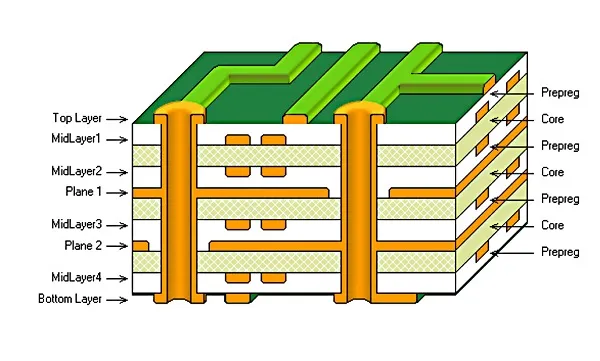
- Via Placement: Optimize via types (through-hole, blind, or buried) to reduce lamination cycles and improve routing density.
For a 4-layer PCB, a typical stack-up might include two signal layers on the outer surfaces, a ground plane, and a power plane, with prepreg layers of 0.15 mm thickness to ensure tight coupling and reduce EMI.
3. Process Parameter Control
Precise control of lamination parameters—temperature, pressure, and time—is essential for consistent results. Recommended settings include:
- Temperature: 180-200°C to fully cure the resin without degrading materials.
- Pressure: 300-500 psi to ensure uniform resin flow and eliminate voids.
- Time: 60-120 minutes, depending on layer count and material properties.
Advanced presses, like the LPKF MultiPress S, use preset profiles to maintain these parameters, reducing defects in high-frequency multilayers. Monitoring the glass transition temperature (Tg, typically 130-180°C for FR-4) ensures the substrate remains stable during lamination.
4. Alignment and Registration Accuracy
Misalignment between layers can cause open circuits or shorts, especially in high-density designs. To optimize alignment:
- Positioning Holes: Use at least three positioning holes for 4-layer boards and five for 6+ layers to ensure precise registration.
- Riveting or Fusing: Employ solder joint positioning or riveting to secure layers before lamination, reducing layer deviation to <0.05 mm.
- Optical Inspection: Use X-ray or automated optical inspection (AOI) post-lamination to detect layer shifts (e.g., deviations >0.1 mm).
For example, Rocket PCB recommends designing overlapping rivet holes for boards with 6+ layers to enhance alignment accuracy.
5. Defect Prevention and Quality Control
Common lamination defects include voids, delamination, and resin starvation. To prevent these:
- Vacuum Lamination: Use a vacuum heat press to remove trapped air, reducing voids by up to 90%.
- Resin Content: Ensure prepreg resin content is sufficient (e.g., 50% for 7628 prepreg) to avoid dry spots.
- Post-Lamination Testing: Conduct thermal stress tests (e.g., 288°C for 10 seconds per IPC-TM-650) to verify bonding strength.
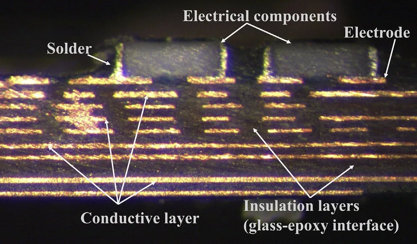
Cross-sectional analysis can reveal defects like white edges (caused by low resin content) or bubbles, allowing process adjustments before full-scale production.
Advanced Techniques for High-Performance PCBs
For high-frequency or high-reliability applications, additional optimization techniques are necessary:
- Sequential Lamination: Build layers sequentially for complex boards (e.g., 12+ layers), allowing precise via filling and reducing warpage.
- Low-Dk Materials: Use materials with low dielectric constants (Dk < 3.5) to minimize signal loss in 5G or RF applications.
- Thermal Management: Incorporate thermal vias (e.g., 0.3 mm diameter, 1 mm pitch) to dissipate heat, improving reliability in power electronics.
These techniques enable boards to support signal speeds up to 10 Gbps while maintaining signal integrity and thermal stability.
How ALLPCB Supports Lamination Optimization
At ALLPCB, we leverage advanced manufacturing capabilities to deliver high-quality multilayer PCBs tailored to your needs. Our state-of-the-art lamination equipment ensures precise control of temperature, pressure, and alignment, minimizing defects and achieving industry-leading tolerances. With support for 4 to 64-layer PCBs and a range of materials (FR-4, Rogers, ceramics), we provide customized solutions for applications from consumer electronics to aerospace. Our rigorous quality control, including AOI and thermal stress testing, guarantees reliable, high-performance boards that meet your exact specifications.
Conclusion
Optimizing the multilayer PCB lamination process is essential for producing reliable, high-performance boards that meet the demands of modern electronics. By focusing on material selection, stack-up design, process control, alignment, and defect prevention, manufacturers can achieve superior results. Advanced techniques like sequential lamination and low-Dk materials further enhance performance for specialized applications. At ALLPCB, we're committed to helping engineers navigate these complexities with cutting-edge solutions and expert support.


