 ALLPCB


If you're dealing with microvia damage on a printed circuit board (PCB), you might be wondering how to fix it effectively. Microvia repair is a specialized process in PCB rework that involves identifying the damage, preparing the area, and applying precise techniques to restore functionality. In this comprehensive guide, we'll walk you through the step-by-step microvia repair process, explore common causes of microvia damage, and provide actionable tips for successful PCB rework. Whether you're an engineer or a technician, this post will equip you with the knowledge to handle microvia replacement and repair with confidence.
What Are Microvias and Why Do They Matter in PCBs?
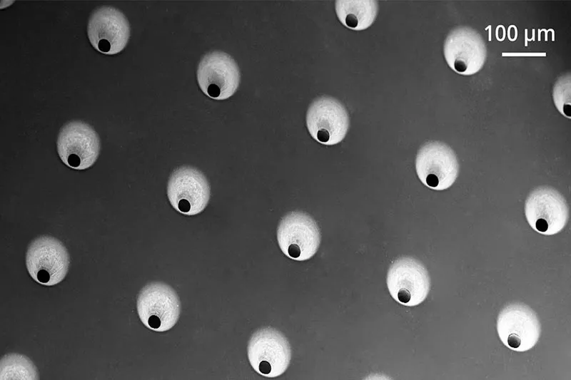
Microvias are tiny holes in a PCB that connect different layers of the board, enabling high-density interconnects (HDI). Typically, these vias have a diameter of less than 150 micrometers (0.15 mm) and are often created using laser drilling for precision. They play a critical role in modern electronics, where space is limited, and component density is high. Microvias allow for faster signal transmission and reduced impedance, often achieving signal speeds up to 10 Gbps or more in advanced designs, depending on the material and layout.
However, due to their small size and the complex manufacturing process, microvias are prone to damage during production or use. Issues like cracking, incomplete plating, or delamination can disrupt the electrical connection, leading to board failure. Understanding microvia repair techniques is essential for maintaining the reliability of high-performance PCBs.
Common Causes of Microvia Damage
Before diving into the microvia repair process, it's important to understand why damage occurs. Identifying the root cause can help prevent future issues during PCB rework. Here are some frequent culprits:
- Thermal Stress: Repeated heating and cooling cycles during soldering or operation can cause microvias to crack. For instance, temperatures exceeding 260°C during reflow soldering can stress the via walls if the board material isn't optimized for high heat.
- Manufacturing Defects: Incomplete copper plating inside the microvia or poor laser drilling can lead to weak connections. Studies suggest that up to 5% of microvias in HDI PCBs may have plating defects if quality control is inadequate.
- Mechanical Stress: Physical handling or bending of the PCB can fracture microvias, especially in flexible or thin boards.
- Environmental Factors: Moisture or chemical exposure can corrode the copper inside microvias, leading to signal loss or open circuits.
Recognizing these issues early can save time and cost during PCB rework. Now, let's explore how to tackle microvia damage with effective repair techniques.
Step-by-Step Microvia Repair Process
The microvia repair process requires precision, patience, and the right tools. Below is a detailed guide to help you through each stage of PCB rework for microvia damage.
Step 1: Assess the Damage
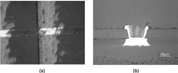
Start by inspecting the PCB to confirm microvia damage. Use a high-powered microscope or X-ray imaging to examine the vias for cracks, voids, or delamination. For example, a crack in the via wall might only be visible at 50x magnification. Document the location and extent of the damage to plan the repair. If the microvia is completely non-functional, you may need to consider microvia replacement rather than a simple fix.
Step 2: Prepare the Work Area
Clean the area around the damaged microvia to remove dust, debris, or oxidation. Use isopropyl alcohol (at least 90% concentration) and a soft brush to gently clean the surface. Ensure the PCB is secured on a stable, anti-static workbench to prevent further damage. Wear an anti-static wrist strap to avoid electrostatic discharge (ESD), which can harm sensitive components.
Step 3: Remove Damaged Material
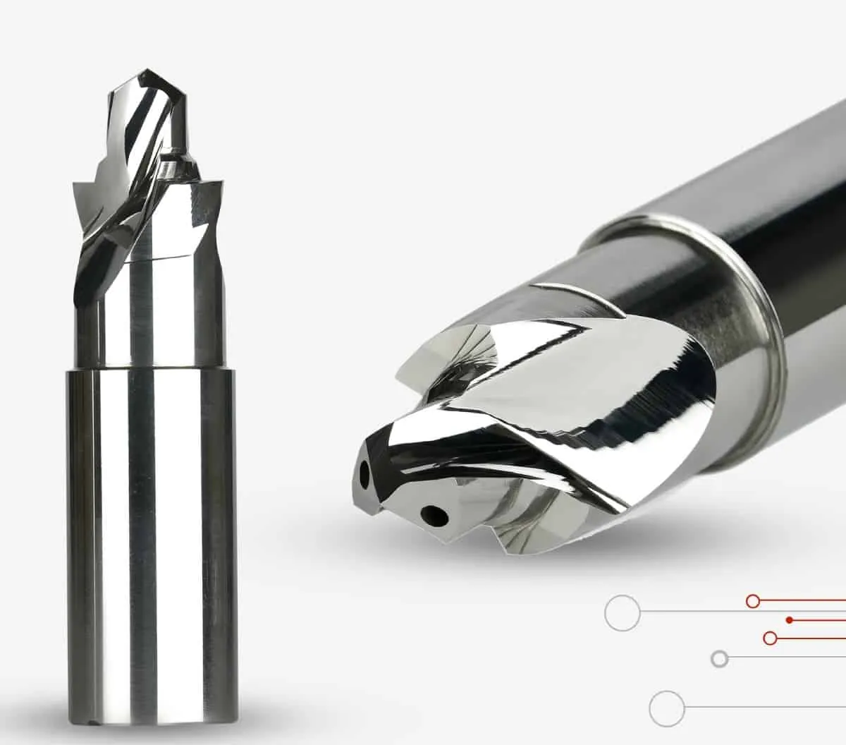
If the microvia is cracked or has poor plating, you may need to remove the damaged section. Use a micro-drill or a precision rotary tool with a bit size smaller than 0.1 mm to carefully clear out the via. Be cautious not to enlarge the hole beyond its original diameter, as this can affect the board's impedance, potentially increasing it by 10-15% if the via geometry changes.
Step 4: Replate or Fill the Microvia
Once the damaged material is removed, the microvia needs to be replated with copper to restore conductivity. This can be done using an electroplating solution or conductive epoxy for smaller repairs. For electroplating, apply a thin layer of copper (approximately 25 micrometers thick) to the via walls using a low-current setup (around 1-2 amps per square decimeter) to ensure even deposition. If using conductive epoxy, apply it with a fine-tip applicator and cure it as per the manufacturer's instructions,
Step 5: Test the Repair
After replating or filling, test the microvia for continuity using a multimeter. Set the multimeter to the lowest resistance range (e.g., 200 ohms) and check if the connection between layers is restored. Ideally, the resistance should be less than 1 ohm for a properly repaired microvia. Additionally, perform a signal integrity test if the PCB handles high-speed signals, ensuring minimal deviation (less than 5%) from the original impedance value, often around 50 ohms for standard designs.
Step 6: Finalize and Protect
Once the repair passes testing, apply a thin layer of solder mask or conformal coating over the repaired area to protect it from environmental damage. Use a UV-curable solder mask for precision, curing it under a UV lamp for about 10-15 seconds. This step helps prevent corrosion and ensures long-term reliability.
Microvia Replacement: When Repair Isn't Enough
In some cases, microvia damage is too severe for a simple repair, and replacement becomes necessary. Microvia replacement involves drilling out the old via entirely and creating a new one, often requiring advanced equipment like a laser drill for precision. Here's a brief overview of the process:
- Drill Out the Damaged Via: Use a laser drill to remove the old microvia, ensuring the hole diameter remains consistent (e.g., 100 micrometers).
- Create a New Via: Re-drill the via if needed and apply copper plating to the walls, following the same electroplating process as in repair.
- Connect and Test: Reconnect the layers and test for continuity and signal integrity as described earlier.
Replacement is more time-consuming and costly than repair, so it should be reserved for cases where the microvia is completely non-functional or poses a risk to the board's performance.
Tools and Materials for Microvia Repair and PCB Rework
Having the right tools is crucial for successful microvia repair and PCB rework. Here's a list of essential items:
- High-Powered Microscope: For inspecting microvias at magnifications of 50x or higher.
- Micro-Drill or Rotary Tool: For removing damaged material, with bit sizes under 0.1 mm.
- Electroplating Kit: For replating copper inside the via, including a power supply and plating solution.
- Conductive Epoxy: As an alternative to plating for small repairs.
- Multimeter: For testing continuity and resistance post-repair.
- Anti-Static Equipment: Including wrist straps and mats to prevent ESD damage.
Investing in quality tools can make the difference between a successful repair and further damage to the PCB.
Tips for Preventing Microvia Damage During PCB Rework
While knowing how to repair microvias is valuable, preventing damage in the first place is even better. Here are some practical tips to minimize the risk of microvia damage during PCB rework:
- Use Proper Materials: Choose PCB substrates with low thermal expansion coefficients (e.g., less than 15 ppm/°C) to reduce stress on microvias during heating.
- Control Soldering Temperatures: Keep reflow soldering temperatures below 260°C and use a controlled heating profile to avoid thermal shock.
- Handle with Care: Avoid excessive bending or mechanical stress on the PCB during handling or assembly.
- Regular Inspections: Perform routine checks using X-ray or microscopic analysis to catch early signs of microvia damage.
Challenges in Microvia Repair and How to Overcome Them
Microvia repair isn't without its challenges, especially given the small scale and precision required. Here are some common hurdles and solutions:
- Challenge: Limited Visibility - Microvias are tiny, making it hard to spot damage or assess repair quality. Solution: Use advanced imaging tools like X-ray systems to see internal defects without damaging the board.
- Challenge: Risk of Over-Drilling - Drilling too deep or wide can ruin the via geometry. Solution: Use a depth-controlled micro-drill and work in small increments, checking progress frequently.
- Challenge: Signal Integrity Issues - Repairs can alter impedance, affecting high-speed signals. Solution: Test impedance post-repair using a time-domain reflectometer (TDR) to ensure it stays within 5% of the target value (e.g., 50 ohms).
Conclusion: Mastering Microvia Repair for Reliable PCB Rework
Microvia repair is a critical skill for anyone involved in PCB rework, especially as electronics continue to shrink in size and increase in complexity. By following the detailed microvia repair process outlined in this guide—assessing damage, preparing the area, replating or replacing the via, and testing the results—you can restore functionality to damaged boards with precision. Additionally, understanding the causes of microvia damage and taking preventive measures can save time and resources in the long run.
Whether you're dealing with a single damaged microvia or planning a full-scale PCB rework project, the techniques and tips provided here will help you achieve reliable results. With the right tools, a steady hand, and attention to detail, microvia repair becomes a manageable task that ensures the longevity and performance of your electronic designs.


