 ALLPCB


If you're an electrical engineer looking to understand how laser PCB depaneling can improve your production process, you're in the right place. Laser PCB depaneling offers high precision cutting with minimal heat affected zone (HAZ), ensuring cleaner cuts, reduced material damage, and enhanced efficiency compared to traditional mechanical methods. In this blog, we’ll dive deep into the advantages of laser PCB depaneling, explore how it minimizes HAZ, compare different laser depaneling machines, and discuss specific technologies like UV laser depaneling and solutions from industry leaders like Coherent. Let’s get started with everything you need to know to optimize your PCB manufacturing process.
What Is Laser PCB Depaneling and Why Does It Matter?
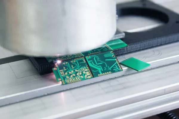
Laser PCB depaneling is a cutting-edge process used to separate individual printed circuit boards (PCBs) from a larger panel during manufacturing. Unlike traditional mechanical methods like routing or sawing, laser depaneling uses focused laser beams to cut through materials with extreme precision. This technology is especially critical for modern electronics, where PCBs are becoming smaller, thinner, and more complex.
For electrical engineers, the shift to laser depaneling matters because it directly impacts the quality and reliability of the final product. Mechanical cutting often causes stress, microcracks, or burrs on the PCB edges, which can lead to failures in high-density or flexible circuits. Laser depaneling, on the other hand, offers a non-contact process that reduces these risks, making it ideal for delicate materials and intricate designs.
Laser PCB Depaneling Advantages for Engineers
The advantages of laser PCB depaneling make it a game-changer for engineers working on high-precision electronics. Let’s break down the key benefits:
- High Precision: Laser systems can achieve cutting accuracies as tight as ±25 micrometers, ensuring exact separation of PCBs without damaging nearby components. This is crucial for applications like wearable devices or medical electronics where tolerances are incredibly small.
- No Mechanical Stress: Since there’s no physical contact, laser depaneling eliminates the risk of mechanical stress or vibration that can crack delicate substrates or dislodge components.
- Versatility: Lasers can cut through a wide range of materials, from rigid FR4 boards to flexible polyimide circuits, without needing to change tools.
- Cleaner Cuts: Unlike mechanical methods that leave burrs or debris, laser cutting produces smooth edges, reducing the need for post-processing and lowering production costs.
- Speed and Efficiency: Modern laser systems can process multiple panels simultaneously at speeds up to 100 mm/s for thin materials, significantly boosting throughput in high-volume production.
For engineers, these advantages translate to fewer design constraints and higher reliability in the field. Imagine working on a flexible PCB for a smartphone—laser depaneling ensures the delicate traces remain intact, preventing signal integrity issues that could arise from mechanical damage.
Understanding Laser Depaneling Heat Affected Zone (HAZ)
One of the biggest concerns when using lasers for PCB cutting is the heat affected zone (HAZ)—the area around the cut where heat from the laser alters the material properties. Excessive HAZ can lead to charring, discoloration, or weakened material, which is unacceptable for high-reliability applications like aerospace or automotive electronics.
However, advancements in laser technology have significantly reduced HAZ. For instance, using short-pulse lasers (like picosecond or femtosecond lasers) minimizes heat transfer to surrounding areas by delivering energy in extremely short bursts. Studies show that HAZ with these lasers can be limited to less than 10 micrometers, compared to 50-100 micrometers with older CO2 lasers.
Additionally, the choice of laser wavelength plays a role. UV lasers, for example, operate at shorter wavelengths (around 355 nm), which are absorbed more efficiently by PCB materials, reducing thermal spread. This makes them ideal for cutting thin or heat-sensitive materials with minimal HAZ. Engineers can further optimize results by adjusting parameters like pulse duration, power (typically 10-20 W for UV lasers), and cutting speed to balance precision and thermal impact.
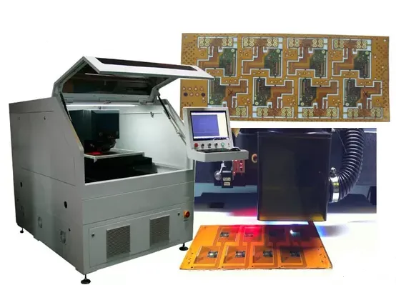
Laser Depaneling Machine Comparison: Finding the Right Fit
Choosing the right laser depaneling machine is critical for achieving the desired precision and minimizing HAZ. Let’s compare some common types of machines and their features to help you make an informed decision:
| Machine Type | Laser Type | Typical Power | Cutting Speed | HAZ | Best For |
|---|---|---|---|---|---|
| CO2 Laser Systems | CO2 (10.6 μm wavelength) | 50-200 W | 50-80 mm/s | Moderate (50-100 μm) | Thicker, less sensitive materials like FR4 |
| UV Laser Systems | UV (355 nm wavelength) | 10-20 W | 80-120 mm/s | Minimal (<10 μm) | Thin, flexible, or heat-sensitive PCBs |
| Fiber Laser Systems | Fiber (1.06 μm wavelength) | 20-50 W | 100-150 mm/s | Low (10-30 μm) | High-speed production of standard PCBs |
Key Takeaways from Comparison:
- If you’re working on thin or flexible PCBs, UV laser systems are often the best choice due to their minimal HAZ and high precision.
- For thicker boards or cost-sensitive projects, CO2 lasers might suffice, though they produce a larger HAZ.
- Fiber lasers strike a balance, offering speed and reasonable HAZ control for high-volume manufacturing.
When selecting a machine, also consider factors like software integration for CAD/CAM compatibility, ease of maintenance, and vendor support. For instance, brands like Han’s Laser and LPKF offer UV laser systems with advanced control software that lets engineers fine-tune cutting parameters for specific materials.
UV Laser Depaneling: Precision for Modern Electronics
UV laser depaneling has emerged as the go-to solution for cutting-edge PCB applications. Operating at a wavelength of 355 nm, UV lasers are absorbed more effectively by most PCB materials, including copper, epoxy, and polyimide, compared to longer-wavelength lasers like CO2. This results in a colder cutting process, with HAZ often below 10 micrometers, as mentioned earlier.
For electrical engineers, UV laser depaneling is particularly valuable when working on high-density interconnect HDI PCBs or flexible printed circuits (FPCs). These boards often have trace widths below 50 micrometers and cannot tolerate thermal damage. A practical example is in smartphone manufacturing, where FPCs must be cut with pinpoint accuracy to fit into tight spaces without compromising signal integrity (often requiring impedance control within ±10%).
Moreover, UV laser systems can handle a variety of tasks beyond depaneling, such as drilling microvias or cutting cover layers, making them versatile tools in a production line. Recent advancements, as noted by companies like Han’s Laser, show that UV systems can achieve cutting speeds up to 120 mm/s on materials as thin as 0.1 mm, ensuring both precision and productivity.
Coherent Laser Depaneling: Industry-Leading Solutions
Coherent, a well-known name in laser technology, offers some of the most advanced solutions for PCB depaneling. Their systems, such as the AVIA LX series, are designed to deliver high precision with minimal thermal impact, making them a favorite among engineers working on sensitive electronics. According to resources from Coherent’s website, their lasers leverage short-pulse technology to reduce HAZ, often achieving cuts with thermal damage zones under 5 micrometers.
One standout feature of Coherent laser depaneling systems is their adaptability to different materials and thicknesses. Whether you’re cutting a 0.2 mm flexible circuit or a 1.6 mm rigid board, their systems allow precise control over power and pulse duration (typically adjustable from 1 to 100 kHz). This flexibility ensures consistent results across diverse projects, from consumer electronics to industrial control systems.
For engineers, Coherent’s focus on integrating user-friendly software is also a plus. Their systems often come with tools to import Gerber files directly, simplifying the setup process and reducing errors in complex designs. If you’re considering investing in a high-end depaneling solution, exploring Coherent’s offerings could provide the precision and reliability your production line needs.
Practical Tips for Implementing Laser Depaneling in Your Workflow
Transitioning to laser PCB depaneling requires careful planning to maximize its benefits. Here are some actionable tips for electrical engineers:
- Material Testing: Before full-scale production, test your specific PCB materials with the laser system to determine optimal settings for power, speed, and pulse duration. For example, a 0.8 mm FR4 board might require a 15 W UV laser at 80 mm/s for clean cuts with minimal HAZ.
- Fixture Design: Use custom fixtures to hold PCB panels securely during cutting, preventing movement that could lead to inaccurate cuts or component damage.
- Ventilation and Safety: Laser cutting can produce fumes, especially with epoxy-based materials. Ensure proper ventilation and follow safety protocols to protect your team.
- Regular Maintenance: Keep laser optics clean and calibrated to maintain cutting accuracy. A misaligned laser can increase HAZ or cause uneven cuts.
- Software Optimization: Leverage the machine’s software to simulate cuts and identify potential issues before processing, saving time and materials.
By following these steps, you can integrate laser depaneling into your workflow with minimal disruption while achieving superior results.
Challenges and Considerations in Laser Depaneling
While laser depaneling offers numerous benefits, it’s not without challenges. Engineers should be aware of the following considerations:
- Initial Cost: Laser systems, especially UV or short-pulse models, can cost upwards of $100,000, compared to $10,000-$30,000 for mechanical routers. However, the long-term savings from reduced scrap and rework often justify the investment.
- Material Limitations: Some materials, like highly reflective metals, may require specialized lasers or coatings to ensure effective cutting.
- Learning Curve: Operating laser systems requires training to master parameter adjustments and maintenance, which can temporarily slow down production during the transition.
Addressing these challenges upfront by budgeting for equipment and training can help ensure a smooth adoption of laser depaneling technology.
Conclusion: Why Laser PCB Depaneling Is the Future
Laser PCB depaneling is revolutionizing the way electrical engineers approach PCB manufacturing. With its unmatched precision, minimal heat affected zone, and versatility across materials, it offers a clear advantage over traditional mechanical methods. Whether you’re leveraging UV laser depaneling for delicate flexible circuits or exploring Coherent laser depaneling systems for high-end applications, this technology can elevate your production quality and efficiency.
As PCBs continue to shrink and designs grow more complex, adopting laser depaneling isn’t just an option—it’s becoming a necessity. By understanding the advantages, managing HAZ, and choosing the right machine for your needs, you can stay ahead in the fast-paced world of electronics manufacturing.
Suggested Reading: The Future of PCB Depaneling: Emerging Trends and Technologies


