 ALLPCB


Do you want to save money on HDI PCB manufacturing without sacrificing quality? The secret lies in optimizing sequential lamination processes. In this blog, we’ll dive deep into cost-effective strategies for HDI PCB production, focusing on sequential lamination cost analysis, HDI PCB manufacturing price reduction, and more. Let’s explore how to streamline your fabrication process and cut down on expenses.
High-Density Interconnect (HDI) PCBs are the backbone of modern electronics, enabling smaller, faster, and more powerful devices. However, manufacturing these complex boards often comes with a high price tag. The good news? By optimizing sequential lamination processes, you can achieve significant PCB fabrication cost reduction while maintaining top-notch quality. In this comprehensive guide, we’ll break down the essentials of sequential lamination cost analysis, strategies for optimizing lamination cycles, and tips to manage HDI PCB manufacturing price and PCB material cost effectively.
Whether you’re an engineer designing cutting-edge devices or a procurement manager looking to streamline budgets, this post will provide actionable insights to help you save money and improve efficiency in HDI PCB production.
What is Sequential Lamination in HDI PCB Manufacturing?
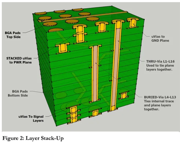
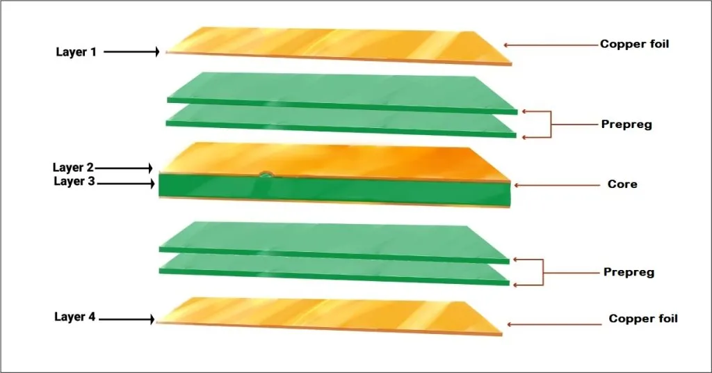
Sequential lamination is a key technique used in the fabrication of HDI PCBs. Unlike traditional PCB manufacturing, which often involves a single lamination step, sequential lamination builds the board layer by layer. Each layer or subset of layers is laminated, drilled, and plated before the next set of layers is added. This process allows for intricate designs with microvias, buried vias, and high-density routing, which are essential for compact and high-performance electronics.
While this method offers unmatched design flexibility, it can also drive up costs due to the multiple cycles of lamination, drilling, and plating. Understanding how to optimize these steps is crucial for PCB fabrication cost reduction.
Why Does HDI PCB Manufacturing Cost So Much?
Before diving into cost-saving strategies, it’s important to understand the factors that contribute to the high HDI PCB manufacturing price. Here are the main culprits:
- Complex Layer Structures: HDI PCBs often have 8, 12, or even 20+ layers, requiring multiple lamination cycles that increase labor and equipment time.
- Specialized Materials: High-frequency and high-performance materials, such as low-loss dielectrics, are often needed, driving up PCB material cost. For instance, materials like Rogers or Isola can cost 30-50% more than standard FR-4.
- Microvia Technology: Creating microvias with laser drilling is precise but expensive, often costing $0.50 to $1.00 per via depending on volume and complexity.
- Tight Tolerances: HDI designs demand precision in impedance control (e.g., maintaining 50 ohms ±10%) and signal integrity, which requires advanced testing and quality control measures.
- Multiple Process Steps: Each sequential lamination cycle adds to the production time, energy use, and potential for defects, all of which increase costs.
By addressing these factors through process optimization and smart material choices, you can significantly lower the overall cost of HDI PCB production.
Sequential Lamination Cost Analysis: Breaking Down Expenses
A detailed sequential lamination cost analysis reveals where expenses accumulate and how to tackle them. Let’s break it down into key areas:
1. Material Costs
PCB material cost is often one of the largest expenses in HDI manufacturing. High-performance laminates and prepregs used in sequential lamination can account for 30-40% of the total board cost. For example, using a high-Tg material (glass transition temperature above 170°C) for thermal stability might cost $5 per square foot, compared to $2 for standard materials.
Cost-Saving Tip: Work with your supplier to identify alternative materials with similar performance characteristics at a lower price. Hybrid stackups, combining high-performance materials only where needed (like in high-frequency signal layers), can reduce costs by up to 20%.
2. Lamination Cycles
Each lamination cycle in sequential lamination adds time and cost. A typical 12-layer HDI board might require 3-4 separate lamination steps, with each cycle costing $50-100 per panel in equipment and labor, depending on the facility’s efficiency.
Cost-Saving Tip: Minimize the number of lamination cycles by designing stackups that group layers efficiently. For instance, combining multiple subsets into a single lamination step, where design rules allow, can cut costs by 10-15%.
3. Drilling and Plating
Laser drilling for microvias and subsequent plating are costly due to precision requirements. A single panel with 1,000 microvias might incur drilling costs of $500 or more.
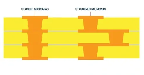
Cost-Saving Tip: Optimize via placement to reduce the total number of microvias. Using staggered vias instead of stacked vias can also lower drilling complexity and cost by around 5-10%.
Strategies for Optimizing Lamination Cycles in HDI PCB Manufacturing
Optimizing lamination cycles is a powerful way to achieve PCB fabrication cost reduction. Here are proven strategies to streamline the process:
1. Design for Fewer Lamination Steps
By carefully planning the PCB stackup, you can reduce the number of sequential lamination cycles. For example, a 10-layer board designed with 2 lamination cycles instead of 3 can save approximately $30-50 per panel in production costs, based on typical industry rates.
How to Do It: Group layers into larger subsets during the design phase. Ensure that signal integrity and thermal performance aren’t compromised by simulating the design with tools that model impedance (e.g., maintaining 100 ohms for differential pairs) and heat dissipation.
2. Use Balanced Stackups
Unbalanced stackups can lead to warping during lamination, increasing defect rates and requiring additional cycles or rework. A balanced stackup, with symmetrical layer distribution, minimizes stress and can reduce defect-related costs by up to 8%.
How to Do It: Ensure copper distribution is even across layers. For instance, if a layer has 70% copper coverage, adjacent layers should be designed with similar coverage to avoid uneven thermal expansion.
3. Leverage Automation in Lamination
Modern manufacturing facilities often use automated lamination systems that reduce human error and speed up cycles. Automation can cut lamination time by 15-20%, directly impacting the HDI PCB manufacturing price.
How to Do It: Partner with a manufacturer that invests in automated equipment. While initial setup costs may be higher, the long-term savings in high-volume production are substantial.
Managing PCB Material Cost Without Compromising Quality
Material selection plays a huge role in controlling expenses. Here’s how to manage PCB material cost effectively:
1. Choose Cost-Effective Dielectrics
High-frequency materials are often necessary for HDI PCBs to maintain signal speeds (e.g., supporting data rates of 10 Gbps or higher). However, using premium materials across all layers is unnecessary. A hybrid approach—using high-performance dielectrics only on critical signal layers—can reduce material costs by 15-25%.
Example: For a board operating at 5 GHz, use a low-loss dielectric with a dissipation factor of 0.002 on signal layers, while standard FR-4 with a dissipation factor of 0.02 can suffice for power and ground planes.
2. Optimize Copper Thickness
Thicker copper layers improve current-carrying capacity but increase costs. For instance, 2 oz copper costs about 20% more per square foot than 1 oz copper. Use thicker copper only where high current is needed, such as power traces, and thinner copper elsewhere.
Example: A power trace carrying 5A might require 2 oz copper for thermal management, while signal traces handling low current can use 0.5 oz copper to save on material.
Additional Tips for PCB Fabrication Cost Reduction
Beyond sequential lamination and material choices, here are broader strategies to lower costs in HDI PCB manufacturing:
- Panel Utilization: Maximize the number of boards per panel to reduce waste. For example, fitting 10 small boards on a 12” x 18” panel instead of 8 can lower per-unit costs by 20%.
- Volume Production: Higher order quantities often come with bulk discounts. Producing 1,000 units instead of 100 can reduce per-board cost by 30-40% due to economies of scale.
- Simplify Testing Requirements: While testing for impedance and signal integrity is critical, over-specifying tests can inflate costs. Limit advanced testing (e.g., TDR for time-domain reflectometry) to only high-risk designs, saving $10-20 per board.
Partnering for Cost-Effective HDI PCB Solutions
Collaborating with an experienced manufacturing partner can make a big difference in achieving cost savings. Look for a provider that offers design-for-manufacturability (DFM) feedback to identify cost-saving opportunities early in the design phase. A good partner will help optimize stackups, suggest alternative materials, and streamline lamination cycles to balance quality and cost.
Additionally, transparency in pricing and process capabilities ensures you’re not hit with unexpected fees. A reliable manufacturer will provide a clear breakdown of costs, from material selection to lamination and testing, helping you make informed decisions.
Conclusion: Balancing Cost and Quality in HDI PCB Manufacturing
Cost-effective HDI PCB manufacturing is achievable by focusing on sequential lamination cost analysis, optimizing lamination cycles, and making smart choices to manage PCB material cost. By designing for fewer lamination steps, using balanced stackups, selecting cost-effective materials, and partnering with the right manufacturer, you can significantly reduce the HDI PCB manufacturing price without compromising performance.
Implementing these strategies can lead to savings of 10-30% on production costs, allowing you to allocate resources to innovation and growth. Start by reviewing your current designs and processes to identify areas for improvement, and take the first step toward more efficient and affordable HDI PCB fabrication today.


