 ALLPCB


In the world of high-reliability electronics, cleanliness isn’t just a preference—it’s a necessity. For industries like aerospace and medical devices, even the smallest residue on a printed circuit board (PCB) can lead to failures, compromising safety and performance. So, how do you ensure your PCBs are impeccably clean and ready for critical applications? Advanced PCB cleaning techniques go beyond basic brushing, incorporating precise methods, strict process control, and thorough validation to meet stringent standards.
In this comprehensive guide, we’ll dive deep into the best practices for cleaning PCBs, focusing on specialized approaches for aerospace and medical applications. We’ll explore PCB cleaning validation, process control, and residue testing to help you achieve the highest reliability. Whether you’re an engineer or a manufacturer, this blog will equip you with actionable insights to elevate your PCB cleaning game.
Why PCB Cleaning Matters for High-Reliability Electronics
PCBs are the backbone of modern electronics, and in high-stakes fields like aerospace and medical devices, their performance can’t be compromised. Residues such as flux, solder paste, dust, or ionic contaminants left on a PCB after manufacturing can cause corrosion, short circuits, or signal interference. For instance, in aerospace systems, a single failure due to contamination could disrupt communication or navigation, leading to catastrophic results. Similarly, in medical devices, residue could affect the precision of life-saving equipment like pacemakers or diagnostic tools.
Cleaning PCBs isn’t just about aesthetics; it’s about ensuring long-term reliability. Studies show that up to 30% of PCB failures in critical applications are linked to contamination. By mastering advanced cleaning techniques, you can reduce failure rates, extend the lifespan of your electronics, and meet industry standards like IPC-6012 for aerospace or ISO 13485 for medical devices.
Advanced PCB Cleaning Techniques for Optimal Results
Traditional cleaning methods like manual brushing with isopropyl alcohol are often insufficient for high-reliability electronics. Advanced techniques provide more consistent and thorough results, ensuring no residue is left behind. Let’s explore some of the most effective methods used in the industry.
1. Ultrasonic Cleaning for Precision
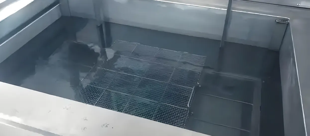
Ultrasonic cleaning uses high-frequency sound waves to create microscopic bubbles in a cleaning solution. These bubbles implode near the PCB surface, dislodging contaminants even from hard-to-reach areas like under components or between tight traces. This method is particularly effective for removing stubborn flux residues and fine particles.
For best results, use a cleaning solution tailored to the type of residue—aqueous solutions for ionic contaminants or solvent-based options for organic residues. The process typically operates at frequencies between 20 kHz and 40 kHz, with cleaning times ranging from 5 to 15 minutes depending on the contamination level. However, care must be taken to avoid damaging delicate components, as excessive power or duration can cause mechanical stress.
2. Vapor Degreasing for Deep Cleaning
Vapor degreasing is a powerful method for removing organic contaminants like oils and greases. It involves heating a solvent to create vapor, which condenses on the cooler PCB surface, dissolving residues and dripping off. This technique is ideal for aerospace PCBs where precision and cleanliness are paramount, as it leaves no water spots or secondary residues.
Common solvents used in vapor degreasing include hydrofluoroethers (HFEs) due to their low toxicity and environmental impact. The process is highly efficient, often completing in under 10 minutes per batch, and is suitable for high-volume production environments.
3. Plasma Cleaning for Surface Preparation
Plasma cleaning uses ionized gas to remove organic contaminants and activate the PCB surface for better adhesion during subsequent processes like conformal coating. This method is especially valuable in medical device manufacturing, where surface cleanliness directly impacts biocompatibility and coating integrity.
Plasma cleaning operates in a vacuum chamber with gases like oxygen or argon, targeting residues at a molecular level. It’s a dry process, meaning there’s no risk of liquid damage to sensitive components, and it can achieve cleanliness levels down to 0.1 nanometers of residue thickness—a critical factor for high-reliability applications.
PCB Cleaning Process Control: Ensuring Consistency
Advanced cleaning techniques are only effective if they’re applied consistently. PCB cleaning process control involves defining parameters, monitoring performance, and maintaining equipment to ensure repeatable results. Without strict control, even the best cleaning method can fail to meet standards for aerospace or medical applications.
Key Elements of Process Control
- Standard Operating Procedures (SOPs): Develop detailed SOPs for each cleaning method, specifying solution types, temperatures, durations, and equipment settings. For example, ultrasonic cleaning might require a solution temperature of 40°C to optimize contaminant removal without degrading the PCB.
- Equipment Calibration: Regularly calibrate cleaning equipment to maintain accuracy. An uncalibrated ultrasonic cleaner, for instance, might operate at inconsistent frequencies, leading to uneven cleaning.
- Environmental Monitoring: Control factors like humidity and temperature in the cleaning area to prevent secondary contamination. A cleanroom environment with humidity below 50% is often recommended for high-reliability PCB production.
By integrating these controls, manufacturers can achieve defect rates as low as 0.01% in cleaned PCBs, a critical benchmark for industries where failure isn’t an option.
PCB Cleaning Validation: Proving Cleanliness Standards
Cleaning a PCB is only half the battle; you must validate that it meets cleanliness standards. PCB cleaning validation ensures that no harmful residues remain, protecting the board’s performance and reliability. This is especially crucial for aerospace and medical devices, where regulatory compliance is non-negotiable.
Common Validation Methods
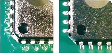
- Visual Inspection: Use high-magnification microscopes (up to 100x) to check for visible residues like flux or particles. While this method is basic, it’s a starting point for identifying major contamination.
- Ionic Contamination Testing: Measure ionic residues using a resistivity of solvent extract (ROSE) test. This test quantifies ionic content in micrograms per square centimeter, with acceptable levels often below 1.56 μg/cm2 per IPC standards for high-reliability electronics.
- Surface Insulation Resistance (SIR) Testing: Assess the PCB’s electrical performance by measuring insulation resistance between traces. A drop in resistance (below 10^8 ohms) can indicate residual contamination affecting signal integrity.
Validation isn’t a one-time step; it should be conducted on a sample basis across production batches to ensure ongoing compliance. For aerospace applications, validation often aligns with MIL-STD-883 standards, while medical devices may follow ISO 10993 for biocompatibility.
Cleaning PCBs for Aerospace: Meeting Stringent Standards
Aerospace electronics operate in extreme conditions—high altitudes, temperature swings, and vibrations. Cleaning PCBs for aerospace requires methods that eliminate all residues to prevent failures in systems like avionics or satellite controls. Even a small short circuit caused by flux residue could disrupt signals traveling at speeds up to 3 GHz in modern communication systems.
Techniques like vapor degreasing and plasma cleaning are often preferred in aerospace due to their ability to achieve near-perfect cleanliness. Additionally, process control must account for the use of specialized materials like high-frequency laminates, which may require specific cleaning solutions to avoid surface damage. Post-cleaning validation typically involves rigorous testing to ensure impedance values remain within tight tolerances, often as precise as ±5% of the design specification.
Cleaning PCBs for Medical Devices: Prioritizing Safety
In medical devices, PCB cleanliness directly impacts patient safety. Residues can interfere with the accuracy of sensors in devices like glucose monitors or cause failures in implantable electronics. Cleaning PCBs for medical devices often involves aqueous-based ultrasonic cleaning to remove biocompatible residues, followed by plasma cleaning to prepare surfaces for coatings that prevent corrosion in bodily environments.
Validation in this sector focuses on biocompatibility, ensuring no toxic residues remain. Standards like ISO 13485 require detailed documentation of cleaning processes, while residue testing often targets organic contaminants that could trigger adverse reactions. Achieving cleanliness levels with less than 0.1 μg/cm2 of ionic residue is a common benchmark for medical-grade PCBs.
Residue Testing After PCB Cleaning: Closing the Loop
Residue testing after PCB cleaning is the final step to confirm that your process has worked. Beyond ionic contamination and SIR testing, advanced methods like Fourier Transform Infrared Spectroscopy (FTIR) can identify specific organic residues at a molecular level. This is particularly useful for diagnosing failures in high-reliability applications, where knowing the exact contaminant can guide process improvements.
For practical implementation, residue testing should be integrated into quality assurance workflows. Test a statistically significant sample from each batch—often 5-10% of production—and maintain detailed records for traceability. In aerospace, residue levels below 0.5 μg/cm2 are often required, while medical applications may demand even stricter limits to ensure safety.
Best Practices for Sustainable and Effective Cleaning
Achieving high cleanliness levels doesn’t mean sacrificing efficiency or environmental responsibility. Here are some best practices to optimize your PCB cleaning process:
- Use Eco-Friendly Solvents: Opt for non-toxic, biodegradable cleaning solutions to reduce environmental impact without compromising effectiveness.
- Automate Where Possible: Automated cleaning systems improve consistency and reduce human error, especially in high-volume production for aerospace and medical sectors.
- Train Staff Regularly: Ensure your team understands the nuances of cleaning techniques and validation methods to maintain quality standards.
- Recycle Cleaning Solutions: Implement filtration systems to reuse cleaning solvents, cutting costs and minimizing waste.
Conclusion: Elevating Reliability Through Advanced Cleaning
Mastering advanced PCB cleaning techniques is a game-changer for high-reliability electronics. From ultrasonic and vapor degreasing methods to strict PCB cleaning process control and validation, every step plays a vital role in ensuring performance and safety. For industries like aerospace and medical devices, where the stakes couldn’t be higher, investing in proper cleaning and residue testing after PCB cleaning isn’t just smart—it’s essential.
By adopting these practices, you can reduce failure rates, meet rigorous industry standards, and build trust in your products. Clean PCBs are the foundation of reliable electronics, and with the right approach, you can achieve results that stand the test of time. Let’s move beyond the brush and embrace the precision of advanced cleaning for a future of flawless performance.


