 ALLPCB


If you're dealing with a malfunctioning CT scanner, the printed circuit board (PCB) is often at the heart of the issue. In this practical guide, we'll dive into CT scanner PCB failure analysis, offering a detailed PCB troubleshooting guide to help you identify and resolve problems. Whether you're looking into component-level repair, addressing common PCB defects, or diagnosing CT scanner errors, this blog will walk you through actionable steps to get your equipment back in working order.
Introduction to CT Scanner PCB Challenges
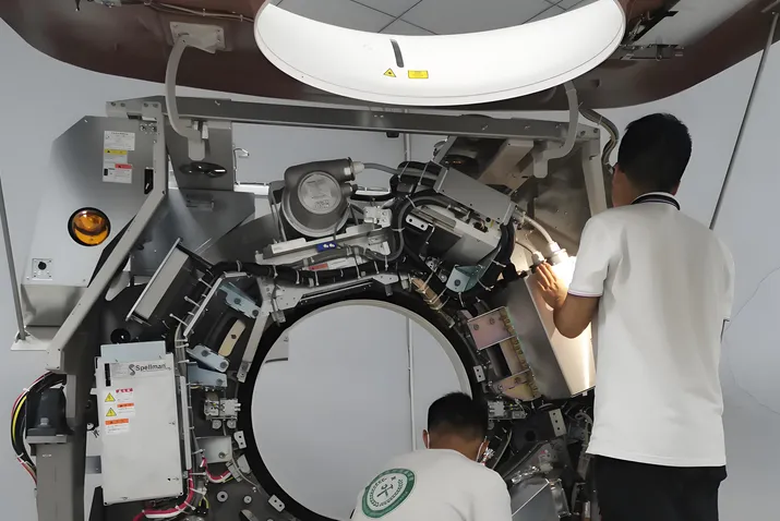
CT scanners are critical tools in medical diagnostics, relying heavily on complex electronic systems. At the core of these systems are PCBs, which control everything from signal processing to power distribution. When a PCB fails, the entire scanner can malfunction, leading to costly downtime and delayed patient care. Understanding how to troubleshoot these boards is essential for technicians and engineers in the medical equipment field.
In this guide, we'll break down the most common issues affecting CT scanner PCBs, provide step-by-step troubleshooting methods, and offer tips for effective repairs. Our goal is to equip you with the knowledge to handle failures efficiently, minimizing disruptions in healthcare settings.
Why Do CT Scanner PCBs Fail?
Before diving into troubleshooting, it's important to understand why PCBs in CT scanners fail. These boards operate in high-stress environments, handling significant electrical loads and continuous operation. Here are some primary reasons for failure:
- Thermal Stress: CT scanners generate heat during operation, which can cause components like capacitors and resistors to degrade over time. Prolonged exposure to temperatures above 85°C can reduce a component’s lifespan by 50% or more.
- Power Surges: Voltage spikes, often exceeding 10-20% of the rated capacity (e.g., a surge from 12V to 15V), can damage sensitive components like microcontrollers.
- Mechanical Stress: Vibrations from moving parts in the scanner can loosen solder joints or crack traces on the PCB.
- Environmental Factors: Dust, humidity levels above 60%, and chemical exposure in hospital settings can corrode board surfaces or lead to short circuits.
- Component Wear: Electrolytic capacitors, for instance, have a finite lifespan, often failing after 5-10 years of use due to electrolyte evaporation.
Recognizing these causes helps narrow down potential issues during CT scanner PCB failure analysis. By identifying the root cause, you can prevent recurring problems and extend the life of the equipment.
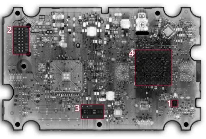
Common PCB Defects in CT Scanners
When it comes to common PCB defects in CT scanners, certain issues appear more frequently. Below, we outline these defects to help you spot them quickly during diagnostics.
1. Solder Joint Failures
Cracked or broken solder joints are a leading cause of PCB issues. These often occur due to thermal expansion or mechanical stress, disrupting the connection between components and the board. Look for visible cracks or components that appear loose.
2. Burnt Components
Overheating or power surges can burn out components like resistors or diodes. A burnt smell or blackened areas on the PCB are clear indicators. For instance, a resistor rated for 0.5W might fail if subjected to a continuous 1W load.
3. Trace Damage
Traces are the copper pathways on a PCB that carry electrical signals. Physical damage or corrosion can break these traces, interrupting signal flow. This is common in high-frequency circuits where signal integrity is critical, often operating at speeds above 100 MHz.
4. Capacitor Leakage or Failure
Electrolytic capacitors can leak or bulge, especially after years of use. A failed capacitor might cause voltage instability, leading to erratic scanner behavior. Check for capacitance values dropping below 80% of their rated specification (e.g., a 100μF capacitor reading only 70μF).
5. Short Circuits
Short circuits occur when unintended connections form between traces or components, often due to solder bridges or debris. This can cause excessive current flow, with amperage spiking beyond safe limits like 2A on a 1A-rated circuit.
Step-by-Step PCB Troubleshooting Guide for CT Scanners
Now that you’re familiar with common issues, let’s explore a structured PCB troubleshooting guide to diagnose and resolve problems. Follow these steps to systematically identify and fix faults.
Step 1: Initial Visual Inspection
Start with a thorough visual check of the PCB. Use a magnifying glass or microscope to look for:
- Discolored or burnt areas.
- Cracked or lifted solder joints.
- Bulging or leaking capacitors.
- Broken traces or visible corrosion.
This non-invasive step often reveals obvious defects without the need for advanced tools.
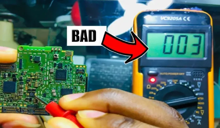
Step 2: Power Supply Testing
Many PCB failures stem from power issues. Use a multimeter to check voltage levels at key points on the board. For example, if a circuit requires 5V but only reads 4.2V, there may be a failing voltage regulator or capacitor. Ensure the power supply is stable within ±5% of the rated value.
Step 3: Signal Integrity Analysis
CT scanners rely on precise signal transmission for imaging accuracy. Use an oscilloscope to measure signal waveforms at critical points. Look for noise or distortion, which could indicate trace damage or interference. Signals should maintain integrity with impedance matched to within 10% of the design specification, often around 50 ohms for high-speed lines.
Step 4: Component Testing
Test individual components using a multimeter or specialized testers. For instance:
- Check resistors for correct ohm values (e.g., a 1kΩ resistor should read close to 1000 ohms).
- Test capacitors for capacitance and leakage.
- Verify diodes and transistors for proper forward and reverse bias behavior.
Replace any component that deviates significantly from its rated specs.
Step 5: Thermal Imaging
Use a thermal camera to detect hot spots on the PCB. Excessive heat, such as a component reaching 100°C when it should operate at 60°C, often indicates a failing part or poor heat dissipation. Address these issues by replacing components or improving cooling.
Step 6: Advanced Diagnostics with CT Scanning
For complex issues, industrial CT scanning can be used to inspect internal PCB structures without disassembly. This non-destructive method helps identify hidden defects like micro-cracks or delamination in multi-layer boards, which are common in CT scanner electronics.
Diagnosing CT Scanner Errors Linked to PCB Issues
When diagnosing CT scanner errors, PCB faults often manifest as specific operational problems. Here’s how to connect symptoms to potential board issues:
- Image Distortion or Artifacts: This could stem from signal integrity issues on the PCB. Check for noise in data acquisition circuits, ensuring signal-to-noise ratios remain above 40 dB.
- Scanner Fails to Power On: Likely a power supply or regulator failure. Test input and output voltages, expecting stable readings like 12V or 24V as per design.
- Intermittent Operation: Often caused by loose solder joints or failing connectors. Inspect for mechanical stress points on the board.
- Error Codes on Display: Many CT scanners log specific error codes tied to PCB failures. Refer to the equipment manual to correlate codes with circuit areas, then test those sections.
By linking symptoms to PCB issues, you can focus your troubleshooting efforts on the most likely culprits, saving time and resources.
Component-Level Repair for CT Scanner PCBs
Once you’ve identified the faulty components through component-level repair techniques, it’s time to fix them. Here’s how to approach repairs safely and effectively:
1. Gather the Right Tools
Ensure you have a soldering iron with fine tips (e.g., 1mm for SMD components), desoldering braid, flux, tweezers, and a steady hand. Anti-static mats and wrist straps are crucial to prevent electrostatic discharge (ESD) damage, which can occur at voltages as low as 100V.
2. Remove Faulty Components
Use desoldering braid or a suction tool to remove old solder. Gently lift the component with tweezers, avoiding damage to nearby traces. For multi-pin components like ICs, work pin by pin to prevent board stress.
3. Clean and Prepare the Area
Clean the pads with isopropyl alcohol (at least 90% purity) and a brush to remove residue. Apply fresh flux to ensure proper solder adhesion.
4. Install New Components
Align the replacement component precisely, then solder each connection. Use minimal solder to avoid bridges—aim for joints that are shiny and concave, indicating a strong bond.
5. Test Post-Repair
After repair, retest the board with a multimeter and oscilloscope to confirm functionality. Power up the scanner to ensure the issue is resolved.
Preventing Future PCB Failures in CT Scanners
While troubleshooting and repairs are essential, preventing failures is equally important. Here are practical steps to extend the life of CT scanner PCBs:
- Regular Maintenance: Schedule quarterly inspections to clean dust and check for early signs of wear, reducing humidity-related corrosion by maintaining levels below 50%.
- Temperature Control: Ensure cooling systems keep PCB temperatures below 70°C during operation.
- Surge Protection: Install surge protectors to limit voltage spikes to within 10% of rated values.
- Quality Components: Use high-grade replacements with matching specifications during repairs to avoid premature failures.
Conclusion: Mastering CT Scanner PCB Troubleshooting
Troubleshooting CT scanner PCB issues doesn’t have to be overwhelming. By following this PCB troubleshooting guide, you can tackle common PCB defects, perform component-level repair, and excel at diagnosing CT scanner errors. From visual inspections to advanced diagnostics like thermal imaging, each step in CT scanner PCB failure analysis brings you closer to a solution.
With the right tools, systematic approaches, and preventive measures, you can keep CT scanners running smoothly, ensuring reliable diagnostics for patients. Bookmark this guide as your go-to resource for handling PCB challenges in medical imaging equipment.


