 ALLPCB


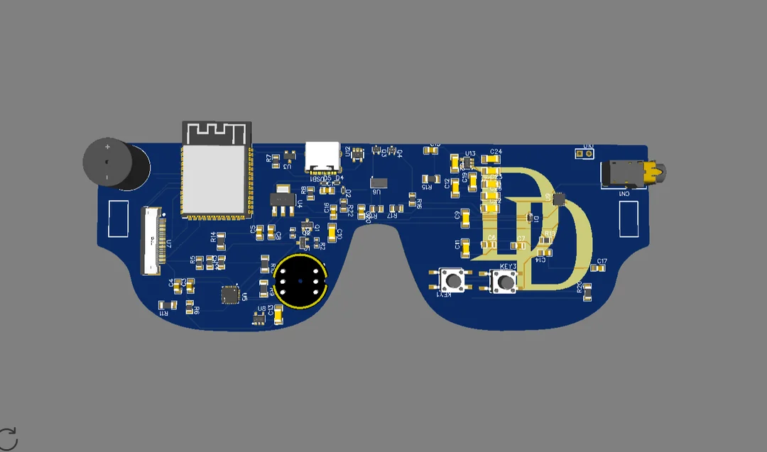
In the fast-evolving world of wearable technology, smart glasses stand out as a groundbreaking innovation. These devices pack incredible functionality into a compact form, requiring highly advanced printed circuit boards (PCBs) to fit within their sleek designs. A key factor in achieving this miniaturization is the use of blind and buried vias in PCB design and manufacturing. But what exactly are blind and buried vias, and how do they contribute to making smart glasses smaller and more efficient? In this blog, we’ll explore their critical role in high-density interconnect (HDI) technology, their impact on smart glasses PCB fabrication, and why they are essential for modern electronics.
What Are Blind and Buried Vias in PCB Design?
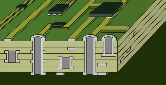
Vias are small holes in a PCB that allow electrical connections between different layers of the board. Traditional through-hole vias go all the way through the PCB, connecting the top and bottom layers. However, in compact devices like smart glasses, space is a premium. This is where blind and buried vias come into play, offering a smarter way to connect layers without wasting valuable real estate.
Blind Vias: These vias connect an outer layer of the PCB to one or more inner layers but do not go through the entire board. For example, a blind via might link the top layer to the second layer, leaving the bottom layers untouched. This saves space on the opposite side of the board for other components or routing.
Buried Vias: These are even more space-efficient, as they connect internal layers of the PCB without reaching either the top or bottom surface. Buried vias are completely hidden within the board, freeing up surface space for additional components or traces.
Both types of vias are crucial in HDI PCB via technology, enabling designers to create smaller, denser boards without sacrificing performance. In smart glasses, where every millimeter counts, these vias are a game-changer.
Why Miniaturization Matters in Smart Glasses PCB Fabrication
Smart glasses integrate a variety of components—processors, sensors, cameras, displays, and batteries—into a lightweight, wearable frame. To achieve this, PCB designers must shrink the board size while maintaining high performance. Miniaturization isn’t just about making things smaller; it’s about optimizing space, reducing weight, and improving signal integrity for faster, more reliable operation.
Traditional PCB designs with through-hole vias often require larger boards because these vias take up space across all layers, even when connections are only needed between specific layers. In contrast, blind and buried vias allow for tighter routing and more efficient use of space. This is especially important in smart glasses, where the PCB must fit into narrow frames or tiny enclosures near the lenses.
For instance, a typical smart glasses PCB might need to handle high-speed signals for augmented reality (AR) displays, requiring signal integrity with minimal interference. Blind vias can reduce signal path lengths by connecting directly to inner layers, cutting down on noise and improving performance. Studies show that shorter signal paths can reduce impedance mismatches by up to 20%, ensuring clearer data transmission at speeds exceeding 5 Gbps.
How Blind Via PCB Design Enhances Smart Glasses
Blind via PCB design plays a pivotal role in the miniaturization of smart glasses by allowing designers to stack more layers in a smaller footprint. In a multilayer PCB, blind vias connect the surface-mounted components (like microchips and sensors) to internal layers without drilling through the entire board. This approach has several benefits:
- Space Savings: By not penetrating all layers, blind vias free up space on the opposite side of the board for other traces or components. In smart glasses, this might mean room for a larger battery or additional sensors.
- Improved Routing Density: Blind vias enable finer trace widths and spacing, often as small as 0.1 mm, allowing more connections in a confined area.
- Better Signal Performance: Shorter vias reduce signal loss and crosstalk, which is critical for high-speed data transfer in smart glasses applications like real-time AR processing.
In practice, a smart glasses PCB might use blind vias to connect a high-speed processor on the top layer to a power distribution network on an inner layer. This direct connection minimizes the board’s thickness, often reducing it to under 0.8 mm, while maintaining robust electrical performance.
The Importance of Buried Via PCB Manufacturing for HDI Technology
Buried via PCB manufacturing takes miniaturization a step further by hiding connections entirely within the internal layers of the board. This technique is a cornerstone of HDI PCB via technology, as it maximizes surface area for component placement. For smart glasses, where every square millimeter of surface space is critical, buried vias offer unmatched advantages:
- Maximized Surface Space: Since buried vias don’t reach the outer layers, both the top and bottom surfaces remain available for mounting components or routing traces.
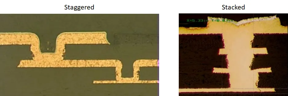
- Support for Complex Designs: Buried vias allow for intricate multilayer designs, often with 6 to 10 layers or more, packed into a board as thin as 0.6 mm.
- Enhanced Reliability: By reducing the number of through-holes exposed to external stress, buried vias lower the risk of mechanical failure in wearable devices that endure frequent movement.
Manufacturing buried vias requires precision, as they are created during the lamination process of the PCB layers. Advanced techniques like sequential lamination ensure that these vias are accurately aligned and filled with conductive material, maintaining strong electrical connections. In smart glasses, buried vias might be used to link internal ground planes for better electromagnetic interference (EMI) shielding, ensuring stable performance even in noisy environments.
Microvia Technology: The Backbone of HDI PCBs in Smart Glasses
Microvia technology is closely tied to blind and buried vias, forming the foundation of HDI PCB designs. Microvias are tiny vias, often less than 0.15 mm in diameter, created using laser drilling for extreme precision. They are typically used as blind or buried vias in HDI boards, enabling ultra-fine connections in compact spaces.
In smart glasses PCB fabrication, microvias are essential for connecting high-density components like micro-LED drivers or wireless communication modules. Their small size allows for pad pitches as tight as 0.4 mm, supporting the integration of advanced chips with hundreds of pins in a tiny area. Additionally, microvias reduce parasitic capacitance and inductance, improving signal integrity for high-frequency applications—think Wi-Fi or Bluetooth signals operating at 2.4 GHz or 5 GHz.
The use of microvias also lowers the overall weight of the PCB, a critical factor for wearable devices. A smart glasses PCB with microvias can weigh as little as 30% less than a traditional board with through-hole vias, making the device more comfortable for prolonged wear.
Challenges in Implementing Blind and Buried Vias for Smart Glasses
While blind and buried vias offer significant advantages, their implementation in smart glasses PCB fabrication comes with challenges. Understanding these hurdles is key to appreciating the expertise required in modern PCB manufacturing.
- Manufacturing Complexity: Creating blind and buried vias involves multiple steps, such as laser drilling for microvias and sequential lamination for buried vias. This increases production time and cost, especially for prototypes.
- Thermal Management: With components packed tightly together, heat dissipation becomes a concern. Blind and buried vias can limit airflow, requiring careful design to prevent overheating in smart glasses, where processors might generate significant heat during AR rendering.
- Reliability Testing: Ensuring the integrity of blind and buried vias under mechanical stress (like bending or vibration in wearables) requires rigorous testing. A failure rate as low as 0.1% can still be catastrophic in consumer electronics.
Despite these challenges, advancements in manufacturing technology are making blind and buried vias more accessible. Automated optical inspection (AOI) systems and X-ray testing now ensure precise via placement and connectivity, reducing defects to near-zero levels in high-quality production environments.
Future Trends in Smart Glasses PCB Fabrication with HDI Technology
As smart glasses continue to evolve, the demand for even smaller, more powerful PCBs will grow. HDI PCB via technology, including blind, buried, and microvias, will remain at the forefront of this transformation. Here are some trends shaping the future:
- Thinner Boards: Advances in materials like ultra-thin laminates will push PCB thicknesses below 0.5 mm, with blind and buried vias enabling denser stacking of layers.
- Integration of AI: Smart glasses with AI-driven features will require faster signal processing, driving the need for microvias with signal speeds exceeding 10 Gbps.
- Sustainable Manufacturing: Eco-friendly fabrication methods, such as lead-free soldering and recyclable materials, will pair with HDI designs to create greener smart glasses without compromising on miniaturization.
These trends highlight the ongoing importance of blind and buried vias in meeting the demands of next-generation wearable tech. As design tools and manufacturing processes improve, the barriers to adopting these technologies will continue to shrink, opening new possibilities for innovation.
Conclusion: The Power of Blind and Buried Vias in Smart Glasses Innovation
The miniaturization of smart glasses would be impossible without the advancements in PCB technology, particularly the use of blind and buried vias. These innovative via types, supported by HDI PCB via technology and microvia technology, allow designers to pack more functionality into smaller spaces while maintaining high performance and reliability. From saving surface area to enhancing signal integrity, blind and buried vias are the unsung heroes behind the sleek, powerful smart glasses we see today.
For engineers and manufacturers, leveraging these technologies in smart glasses PCB fabrication is not just a trend—it’s a necessity to stay competitive in the fast-paced world of wearable electronics. As we look to the future, the role of blind and buried vias will only grow, driving the next wave of innovation in compact, high-performance devices.
At ALLPCB, we’re committed to supporting your journey in creating cutting-edge electronics with state-of-the-art PCB solutions. Whether you’re designing the next big thing in smart glasses or exploring other wearable technologies, our expertise in HDI and advanced via technologies can help bring your vision to life.


