ALLPCB


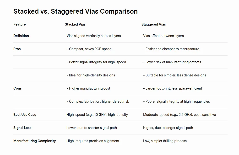
When designing a high-density interconnect (HDI) PCB, one of the critical decisions you’ll face is choosing between stacked and staggered microvias. Both designs play a vital role in connecting layers in compact PCB stackups, but they differ significantly in terms of reliability, cost, and performance. So, which is right for your project? In short, stacked microvia design excels in space-saving and high-density applications but can be costlier and less reliable under thermal stress, while staggered microvia design offers better reliability and lower cost at the expense of more board space.
In this comprehensive guide, we’ll dive deep into the differences between stacked and staggered microvias, exploring their impact on microvia reliability, microvia cost, and suitability for various HDI PCB stackup configurations. By the end, you’ll have a clear understanding of the stacked microvia advantages and disadvantages, as well as those of staggered designs, to make an informed choice for your next PCB project.
What Are Microvias and Why Do They Matter in HDI PCB Design?
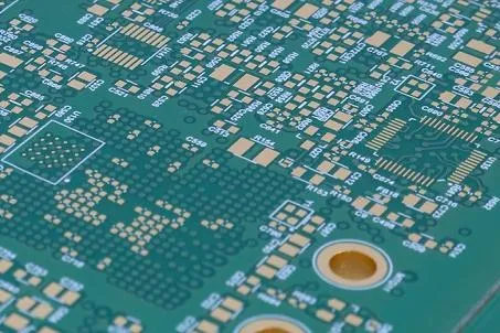
Microvias are small, laser-drilled holes in a PCB that connect adjacent layers, typically with a diameter of less than 150 micrometers. Unlike traditional through-hole vias, microvias enable much higher interconnect density, making them essential for modern HDI designs where space is at a premium. They are commonly used in applications like smartphones, wearables, and other compact electronics that demand intricate multilayer stackups.
In HDI PCB design, microvias reduce the need for larger vias that take up valuable real estate, allowing for finer trace widths and spacing. This results in improved signal integrity, often achieving impedance values as low as 50 ohms for high-speed signals, and faster data transmission rates, sometimes exceeding 10 Gbps in advanced designs. However, the way microvias are arranged—either stacked or staggered—can significantly impact the board’s performance, cost, and manufacturability.
Understanding Stacked Microvia Design
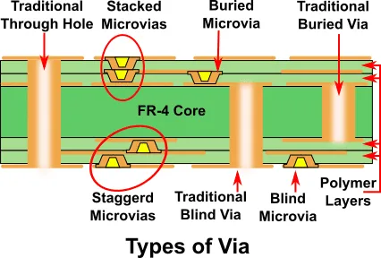
A stacked microvia design involves placing microvias directly on top of each other across multiple layers in an HDI PCB stackup. This vertical alignment creates a straight path for signals to travel through the layers, minimizing the space required for interconnections. Stacked microvias are often used in highly compact designs where every square millimeter counts.
Advantages of Stacked Microvia Design
- Space Efficiency: By stacking microvias vertically, this design allows for tighter routing and smaller board footprints, ideal for ultra-compact devices. For instance, in a 10-layer HDI stackup, stacked microvias can save up to 30% more space compared to staggered configurations.
- Improved Signal Integrity: The direct vertical path reduces signal path length, minimizing inductance and capacitance. This can result in cleaner signals, with signal delays reduced by as much as 10-15% in high-speed applications.
- Higher Density: Stacked microvias enable more connections in a smaller area, supporting complex multilayer designs with up to 16 or more layers in some advanced PCBs.
Disadvantages of Stacked Microvia Design
- Lower Reliability: One of the primary concerns with stacked microvias is microvia reliability. The vertical stacking creates stress points during thermal cycling (e.g., temperature swings from -40°C to 85°C), which can lead to cracks or delamination. Studies have shown failure rates as high as 5-10% in stacked microvias under extreme conditions.
- Higher Cost: Manufacturing stacked microvias requires precise laser drilling and plating processes across multiple layers, increasing microvia cost by 20-40% compared to staggered designs.
- Complex Fabrication: The process of aligning and plating stacked microvias is technically challenging, often requiring advanced equipment and stricter quality control, which can lead to longer lead times.
Exploring Staggered Microvia Design
In contrast, a staggered microvia design positions microvias offset from one another across layers, rather than directly stacked. This means each microvia connects to a small pad or trace on an intermediate layer before continuing to the next layer. Staggered microvias are often chosen for applications where reliability and cost are prioritized over extreme density.
Advantages of Staggered Microvia Design
- Enhanced Reliability: The offset arrangement reduces mechanical stress during thermal expansion, improving microvia reliability. Failure rates for staggered microvias can be as low as 1-2% under similar thermal stress conditions compared to stacked designs.
- Lower Cost: Staggered microvias are easier and less expensive to manufacture since they don’t require the same level of precision as stacked structures. This can reduce microvia cost by up to 30% in large-scale production.
- Easier Fabrication: The offset design simplifies the drilling and plating process, making it more accessible for standard manufacturing setups and reducing the risk of defects.
Disadvantages of Staggered Microvia Design
- Increased Board Space: The offset placement requires more horizontal space for routing between microvias, which can increase the overall board size by 10-20% compared to stacked designs.
- Signal Integrity Challenges: The longer signal paths due to staggered placement can introduce slight delays and higher inductance, potentially affecting high-speed signals above 5 Gbps.
- Limited Density: Staggered microvias are less suitable for extremely dense designs, often limiting their use in ultra-compact applications with more than 12 layers.
Comparing Stacked vs. Staggered Microvias: Key Factors for Your Decision
Choosing between stacked and staggered microvias depends on your project’s specific requirements. Let’s break down the comparison across critical factors like reliability, cost, and application suitability in an HDI PCB stackup.
Microvia Reliability
As mentioned earlier, microvia reliability is a significant concern in HDI designs, especially for applications exposed to temperature fluctuations or mechanical stress. Stacked microvias, while space-efficient, are more prone to failure due to stress concentration at the via interfaces. For example, in automotive or aerospace applications where boards may endure thermal cycles from -55°C to 125°C, failure rates for stacked microvias can spike. On the other hand, staggered microvias distribute stress more evenly, making them a safer choice for reliability-critical designs.
Microvia Cost
Cost is another deciding factor. The microvia cost for stacked designs is higher due to the complexity of manufacturing. For a typical 8-layer HDI board, using stacked microvias might increase production costs by $0.50 to $1.00 per square inch compared to staggered microvias. If you’re working on a high-volume project where cost savings are crucial, staggered microvias offer a more budget-friendly option without sacrificing too much functionality.
Space and Density Requirements
For projects where board size is a constraint, such as in wearable devices or IoT modules, stacked microvias are often the better choice. Their vertical alignment supports higher interconnect density, allowing for finer pitch components like 0.4mm BGA packages. Staggered microvias, while reliable, may not meet the density needs of such compact designs, requiring a larger footprint to achieve the same connectivity.
Signal Integrity and Performance
In high-speed applications, signal integrity is paramount. Stacked microvias provide a shorter signal path, reducing parasitic effects and supporting data rates above 10 Gbps with controlled impedance around 50 ohms. Staggered microvias, due to their longer paths, may introduce minor signal degradation, making them less ideal for cutting-edge high-speed designs unless compensated with careful routing.
Application-Specific Recommendations for HDI PCB Stackup
Your choice of microvia design should align with the specific demands of your application. Here are some tailored recommendations:
- Consumer Electronics (e.g., Smartphones, Tablets): Opt for stacked microvia design to maximize density and minimize board size. The controlled environment of consumer devices often mitigates reliability concerns.
- Automotive and Industrial Applications: Choose staggered microvia design for better reliability under harsh conditions like thermal cycling and vibration.
- High-Speed Networking Equipment: Prioritize stacked microvias to ensure optimal signal integrity for data rates exceeding 5 Gbps, but consider hybrid designs with staggered microvias in less critical areas to balance cost.
- Cost-Sensitive Projects: Use staggered microvias to keep production expenses low, especially for larger boards where space isn’t a critical constraint.
Best Practices for Designing with Microvias
Regardless of whether you choose stacked or staggered microvias, following best practices during the design phase can enhance performance and manufacturability in your HDI PCB stackup.
- Optimize Aspect Ratio: Keep the microvia aspect ratio (depth-to-diameter) below 1:1 to ensure reliable plating and minimize defects. For instance, a 100-micrometer diameter microvia should not exceed 100 micrometers in depth.
- Use High-Quality Materials: Select laminates with low coefficients of thermal expansion (CTE) to reduce stress on microvias during thermal cycles. Materials with CTE values below 15 ppm/°C are ideal.
- Simulate Thermal Performance: Use simulation tools to predict how thermal stress will affect microvia reliability, especially for stacked designs, and adjust the stackup accordingly.
- Work Closely with Manufacturers: Collaborate with your fabrication partner to ensure the chosen microvia design aligns with their capabilities, avoiding costly redesigns or production delays.
Conclusion: Making the Right Choice for Your PCB Design
Deciding between stacked microvia design and staggered microvia design comes down to balancing trade-offs in microvia reliability, microvia cost, and design constraints in your HDI PCB stackup. Stacked microvias shine in high-density, space-constrained applications with a focus on signal integrity, despite their higher cost and potential reliability issues. Staggered microvias, on the other hand, offer a cost-effective and reliable solution for projects where space is less critical and durability is a priority.
By understanding the stacked microvia advantages and disadvantages alongside those of staggered designs, you can tailor your choice to meet the unique needs of your project. Whether you’re designing for consumer electronics, automotive systems, or high-speed networking, the right microvia design will ensure optimal performance and manufacturability for your PCB.
At ALLPCB, we’re committed to supporting your HDI PCB projects with expert guidance and high-quality manufacturing solutions. Evaluate your design goals, consider the factors discussed, and select the microvia structure that best fits your application for a successful outcome.