ALLPCB


If you're looking to design printed circuit boards (PCBs) that balance functionality with manufacturing costs, sizing strategies are key. The right PCB size can reduce material waste, lower fabrication expenses, and optimize production efficiency without sacrificing performance. In this comprehensive guide, we'll explore practical ways to achieve cost-effective PCB sizing, focusing on critical aspects like material costs per square inch, panelization optimization, and minimizing waste. Whether you're working on prototyping or full-scale production, these strategies will help you save money while maintaining quality.
Why PCB Sizing Matters for Cost and Functionality
PCB sizing directly impacts both the cost of manufacturing and the functionality of your design. A board that's too large may waste expensive materials and increase fabrication costs, while a board that's too small might not accommodate all necessary components, leading to performance issues. Striking the right balance requires careful planning and an understanding of how size influences production processes and expenses. Let's dive into actionable strategies to optimize PCB sizing for cost-effectiveness while ensuring your design meets its intended purpose.
Understanding PCB Material Cost per Square Inch
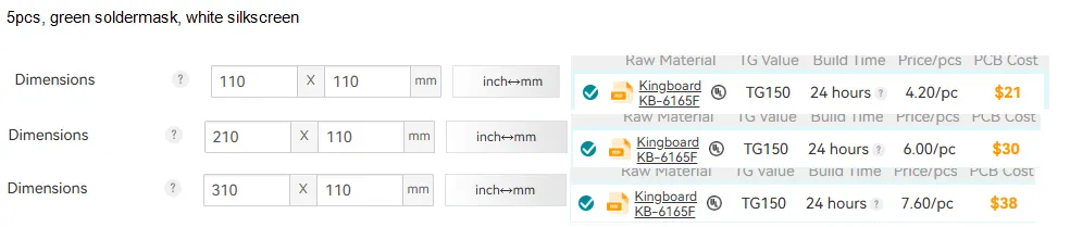
One of the first factors to consider when sizing a PCB is the material cost per square inch. The substrate material, such as FR-4, high-frequency laminates, or metal-core options, significantly affects the overall expense. For instance, standard FR-4, a common choice for many applications, typically costs between $0.10 to $0.50 per square inch for basic designs, depending on thickness and supplier pricing. More specialized materials, like those used for high-frequency or thermal management applications, can cost upwards of $1.00 per square inch or more.
To keep costs down, aim to minimize the board's footprint while ensuring all components fit comfortably. Reducing the size by even a few square inches can lead to substantial savings, especially in high-volume production. However, don't compromise on critical spacing or trace widths—overcrowding can lead to signal interference or manufacturing defects, which may cost more to fix in the long run.
A practical tip is to use design software to simulate different layouts and calculate the exact material area required. By iterating on the design early, you can avoid over-specifying dimensions and keep material costs in check. Additionally, consult with your manufacturing partner to understand their material pricing structure, as bulk discounts or standard sizes may further reduce expenses.
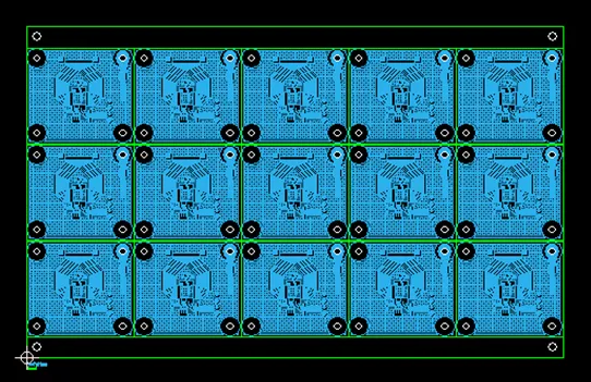
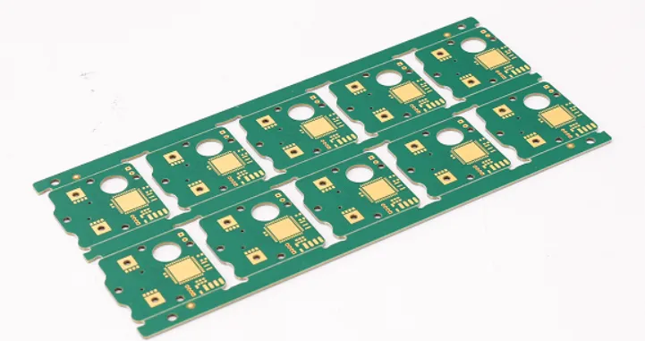
Optimizing PCB Size for Panelization
Panelization is the process of grouping multiple PCBs onto a single manufacturing panel to maximize production efficiency. Optimizing PCB size for panelization is a powerful strategy to lower costs, as it reduces material waste and speeds up fabrication. Manufacturers often work with standard panel sizes, such as 18 x 24 inches or 12 x 18 inches, and fitting as many boards as possible onto these panels can significantly cut down on per-unit costs.
For example, if your PCB measures 2 x 3 inches, arranging 48 boards on an 18 x 24-inch panel uses nearly all available space, minimizing unused material. In contrast, an awkwardly sized board, like 2.5 x 3.2 inches, may only fit 36 units on the same panel, leaving more empty space and increasing waste. To optimize for panelization, design your PCB dimensions to align with standard panel sizes or consult with your manufacturer to understand their preferred configurations.
Another tip is to use uniform shapes whenever possible. Rectangular or square boards are easier to panelize than irregular shapes, which may require additional spacing or custom panel layouts, driving up costs. By focusing on panel-friendly sizing, you can achieve economies of scale and reduce the overall expense of production.
PCB Fabrication Costs for Different Sizes
Fabrication costs vary widely depending on PCB size, as larger boards require more material, longer processing times, and sometimes specialized equipment. For small prototypes, a board under 10 square inches might cost between $5 and $20 to fabricate, while a larger board of 50 square inches could range from $30 to $100 or more, depending on complexity and layer count.
It's also worth noting that many manufacturers charge based on the smallest enclosing rectangle of your design, even if parts of the board are cut out or unused. This means that irregular shapes or oversized outlines can inflate costs unnecessarily. To avoid this, keep your design compact and aligned with standard dimensions that fit efficiently into the manufacturer's pricing tiers.
For high-volume orders, small reductions in size can lead to significant savings. For instance, shrinking a board from 20 square inches to 18 square inches might reduce the per-unit cost by $0.50. Over a run of 10,000 units, that's a savings of $5,000. Always weigh these potential savings against functionality—ensure that size reductions don't compromise critical aspects like component placement or heat dissipation.
Minimizing Waste in PCB Manufacturing
Waste reduction is a cornerstone of cost-effective PCB manufacturing. Material waste not only increases expenses but also impacts the environment, making efficient sizing a priority for sustainable design. One effective way to minimize waste is through careful planning during the design phase. Use software tools to test different layouts and orientations, ensuring that your PCB dimensions make the best use of available panel space.
Another approach is to standardize component sizes and board dimensions across multiple projects. If you frequently design boards of similar sizes, manufacturers can reuse panel setups, reducing setup costs and material offcuts. Additionally, consider using breakaway tabs or mouse bites to separate individual boards from a panel. These small connections allow for tighter packing without wasting material on large gaps or borders.
Finally, communicate with your manufacturing partner about their capabilities and constraints. Some facilities offer advanced nesting algorithms that automatically arrange boards to minimize waste, while others may provide feedback on how to adjust dimensions for better efficiency. By collaborating early in the design process, you can avoid costly revisions and ensure a lean manufacturing workflow.
PCB Prototyping Costs by Size
Prototyping is often the most expensive phase of PCB development on a per-unit basis, especially for small runs where economies of scale don't apply. Prototyping costs are heavily influenced by size, as larger boards require more material and longer fabrication times. For a small prototype under 5 square inches, you might pay $10 to $30 per board for a batch of five. A larger prototype of 20 square inches could cost $50 to $100 per board for the same batch size.
To manage prototyping costs, start with the smallest feasible size that meets your design requirements. If you're testing a specific circuit or feature, consider breaking the design into smaller modules that can be prototyped individually. This approach not only reduces material costs but also allows for faster iteration and debugging.
Another cost-saving tactic is to use online quoting tools to compare pricing for different sizes and quantities. Many manufacturing services offer instant quotes based on your board dimensions, helping you identify the most budget-friendly options. Keep in mind that rush orders or non-standard sizes can add significant premiums to prototyping costs, so plan ahead and stick to common dimensions whenever possible.
Balancing Functionality with Cost in PCB Sizing
While cost reduction is a critical goal, functionality must always take precedence. A PCB that’s too small to support proper trace routing or component spacing can lead to signal integrity issues, such as crosstalk or impedance mismatches. For example, high-speed designs often require specific trace widths and spacing to maintain signal integrity—reducing board size at the expense of these parameters can result in a non-functional product.
Thermal management is another consideration. Larger boards may be necessary to dissipate heat effectively, especially for power-intensive applications. If downsizing a board compromises heat dissipation, you risk component failure or reduced lifespan. In such cases, it’s worth investing in a slightly larger size or exploring alternative materials with better thermal properties, even if the upfront cost is higher.
To strike the right balance, use simulation tools to test how size changes affect electrical and thermal performance. Start with a slightly oversized layout to ensure functionality, then gradually reduce dimensions while monitoring key metrics like signal speed (e.g., ensuring signals propagate at expected speeds of around 8 inches per nanosecond on standard FR-4) and impedance values (e.g., maintaining 50 ohms for controlled impedance lines). This iterative approach helps you find the sweet spot between cost and performance.
Practical Tips for Cost-Effective PCB Sizing
Here are some actionable tips to help you optimize PCB sizing for cost savings without sacrificing functionality:
- Start with a Modular Design: Break complex circuits into smaller, testable sections to reduce prototyping costs and simplify sizing decisions.
- Stick to Standard Dimensions: Align your PCB size with common panel sizes or manufacturer recommendations to avoid custom fees and material waste.
- Use Design Software: Leverage tools to simulate layouts, calculate material usage, and identify opportunities for size reduction.
- Prioritize Component Placement: Arrange components efficiently to minimize board area while maintaining clearance for manufacturing and assembly.
- Collaborate Early: Work with your manufacturing partner during the design phase to understand cost drivers and optimize for their processes.
Conclusion: Achieving Cost-Effective PCB Sizing
Designing a cost-effective PCB requires a thoughtful approach to sizing that balances manufacturing expenses with functional requirements. By focusing on material costs per square inch, optimizing for panelization, understanding fabrication costs for different sizes, minimizing waste, and managing prototyping expenses, you can significantly reduce overall costs. At the same time, always prioritize the performance needs of your design—whether it's maintaining signal integrity, ensuring proper thermal management, or accommodating all necessary components.
With the strategies outlined in this guide, you’re equipped to make informed decisions that save money without compromising quality. Whether you're a hobbyist working on a single prototype or an engineer managing large-scale production, these tips will help you achieve efficient, budget-friendly PCB designs. Remember to leverage design tools, collaborate with manufacturing experts, and iterate on your layouts to find the perfect balance for your next project.