ALLPCB


If you're working on a circuit board and need to remove solder mask to expose copper traces or rework a design, you're in the right place. Solder mask removal is a common task in PCB repair, prototyping, and redesign, and there are several reliable methods to get the job done without damaging the board. In this guide, we'll explore four proven techniques for removing solder mask: grinding and scraping, milling, microblasting, and chemical stripping. Whether you're a hobbyist or a professional engineer, you'll find actionable tips and detailed steps to help you succeed in your circuit board design projects.
At ALLPCB, we understand the challenges of working with PCBs and the importance of precision in every step. Let's dive into these techniques to ensure you can remove solder mask safely and effectively, no matter the complexity of your project.
What Is Solder Mask and Why Remove It?
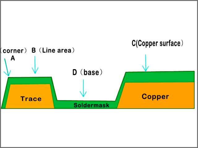
Solder mask is a thin protective layer, usually green, applied to printed circuit boards (PCBs) to insulate copper traces and prevent solder bridges during assembly. It also protects the board from oxidation and environmental damage. However, there are times when you need to remove this layer—whether to access underlying traces for testing, repair a damaged section, or modify the circuit board design.
Removing solder mask can be tricky since it requires precision to avoid damaging the delicate copper traces or the board's substrate. Common reasons for removal include exposing test points, correcting design errors, or salvaging components. The techniques we'll discuss—grinding, scraping, milling, microblasting, and chemical stripping—are widely used in the industry and can be adapted based on the tools you have and the scale of the task.

Technique 1: Grinding and Scraping for Simple Solder Mask Removal
Grinding and scraping is one of the most straightforward and accessible methods for removing solder mask. This technique works best for small areas or when you need a quick fix without specialized equipment. It involves using hand tools like a knife, scraper, or pick to manually remove the mask.
How It Works: The process relies on physically abrading the solder mask layer until the copper beneath is exposed. A skilled technician can control the depth and area of removal by adjusting the pressure and angle of the tool. For tougher masks, a rotary tool with a fine grinding bit can be used to speed up the process.
Steps to Follow:
- Prepare your workspace with proper lighting and magnification if needed to see small details.
- Use a sharp utility knife or scraper to gently score the solder mask over the target area.
- Apply light pressure and scrape in small, controlled motions to avoid gouging the copper traces.
- If using a rotary tool, set it to a low speed (around 5,000-10,000 RPM) and use a fine grinding bit to remove the mask layer by layer.
- Clean the area with isopropyl alcohol and a brush to remove debris.
Pros: This method requires minimal investment since basic tools are often already available. It’s also highly controlled when done by hand, reducing the risk of over-removal.
Cons: Grinding and scraping can be time-consuming for larger areas. There’s also a risk of scratching or damaging the copper if too much force is applied.
Best For: Small repairs or hobbyist projects where precision tools aren’t available.

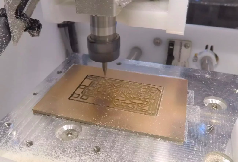
Technique 2: Milling for Precision Solder Mask Removal
Milling is a more advanced technique that uses a high-speed cutting tool to remove solder mask with precision. This method is ideal for professionals or those with access to a workshop equipped with a milling machine or a specialized PCB rework station. It’s particularly effective when you need to remove solder mask from specific areas without affecting surrounding components.
How It Works: A milling machine uses a small, high-speed cutter (often with a diameter of 0.5-1.0 mm) to shave off the solder mask layer. The depth of the cut can be precisely controlled, which is critical to avoid penetrating the board surface or damaging copper traces.
Steps to Follow:
- Secure the PCB firmly in place on the milling machine to prevent movement during the process.
- Select a fine end mill or cutter suited for PCB materials (carbide cutters are often recommended).
- Set the depth control to remove only the solder mask layer, typically 0.1-0.2 mm at a time, depending on the mask thickness.
- Operate the machine at a moderate speed (around 20,000-30,000 RPM) to ensure a clean cut without overheating the board.
- Inspect the area frequently under magnification to ensure you’re not cutting too deep.
- Clean the board with compressed air or a soft brush to remove dust and debris.
Pros: Milling offers excellent precision and is faster than manual scraping for larger or more complex areas. It’s also repeatable, making it suitable for batch rework tasks.
Cons: This method requires specialized equipment and training. There’s also a risk of damaging the board if depth control isn’t properly managed.
Best For: Professional environments or intricate circuit board designs where accuracy is paramount.
Technique 3: Microblasting for Large Area Solder Mask Removal
Microblasting, also known as abrasive blasting, is an excellent technique for removing solder mask from larger areas or when dealing with tough, thick coatings. It uses a stream of fine abrasive particles, such as aluminum oxide or glass beads, propelled by compressed air to strip away the mask without damaging the underlying copper if done correctly.
How It Works: The abrasive particles erode the solder mask layer by layer, exposing the copper beneath. The process can be controlled by adjusting the pressure (typically 40-80 PSI) and the type of abrasive used. A stencil or masking tape can protect areas you don’t want to blast.
Steps to Follow:
- Set up a microblasting unit in a well-ventilated area or blasting cabinet to contain the abrasive material.
- Apply masking tape or a stencil to protect areas of the PCB where solder mask should remain.
- Use a fine abrasive material (50-100 micron particle size) to minimize damage to the copper traces.
- Adjust the air pressure to a low setting (start at 40 PSI) and test on a scrap board to find the right balance.
- Blast the target area in short bursts, checking progress frequently to avoid over-removal.
- Clean the board thoroughly with compressed air and isopropyl alcohol to remove residual abrasive particles.
Pros: Microblasting is fast and effective for large areas. It can also handle various solder mask types and thicknesses with minimal risk to the board if controlled properly.
Cons: This method requires specialized equipment and a controlled environment to manage dust and debris. There’s also a learning curve to avoid damaging delicate traces.
Best For: Larger rework projects or industrial settings where efficiency is key.
Technique 4: Chemical Stripping for Gentle Solder Mask Removal
Chemical stripping is a non-abrasive method that uses specialized chemicals to dissolve the solder mask layer without mechanical force. This technique is ideal when you want to avoid physical stress on the PCB or when working with delicate boards where grinding or milling might cause damage.
How It Works: A chemical stripper, often a solvent-based solution designed for PCB rework, breaks down the polymer structure of the solder mask. The process requires careful handling due to the hazardous nature of the chemicals involved.
Steps to Follow:
- Work in a well-ventilated area and wear protective gear, including gloves and safety glasses, to handle chemicals safely.
- Apply masking tape or a resist material to protect areas of the PCB where solder mask should remain.
- Use a small brush or cotton swab to apply the chemical stripper to the target area, following the manufacturer’s instructions for dwell time (usually 5-15 minutes).
- Gently scrub the softened solder mask with a soft brush or plastic scraper to remove it.
- Rinse the area with isopropyl alcohol or a recommended neutralizer to stop the chemical reaction and clean the board.
- Dispose of chemical waste according to local regulations.
Pros: Chemical stripping is gentle on the PCB and can be used on delicate or thin boards where mechanical methods might cause damage. It’s also effective for irregular shapes or hard-to-reach areas.
Cons: This method involves handling hazardous chemicals, requiring strict safety precautions. It can also be slower than mechanical methods and may not work on all types of solder mask.
Best For: Delicate boards or small, intricate areas where mechanical removal isn’t feasible.
Tips for Safe and Effective Solder Mask Removal
No matter which technique you choose, following best practices ensures the best results and protects your circuit board design from damage. Here are some key tips to keep in mind:
- Always Use Magnification: A magnifying glass or microscope helps you see fine details and avoid over-removal or damage to copper traces.
- Work Slowly: Rushing can lead to mistakes. Take your time to check progress frequently, especially with mechanical methods like grinding or milling.
- Protect Surrounding Areas: Use masking tape or other barriers to shield parts of the PCB you don’t want to affect during removal.
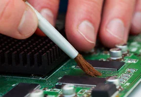
- Clean Thoroughly: After removal, clean the board with isopropyl alcohol (90% or higher concentration) to remove debris, dust, or chemical residues that could interfere with soldering or testing.
- Test Continuity: After exposing copper traces, use a multimeter to check for continuity and ensure no traces were damaged during the process.
Choosing the Right Technique for Your Project
Each of these four techniques—grinding and scraping, milling, microblasting, and chemical stripping—has its strengths depending on the scope of your project and the tools at your disposal. For quick, small-scale fixes in circuit board design, grinding and scraping might be enough. For precision tasks or professional rework, milling offers unmatched control. Microblasting excels in larger areas, while chemical stripping is the go-to for delicate boards where mechanical stress must be avoided.
Consider factors like the size of the area, the type of solder mask (some are thicker or more resistant), and your access to equipment. Safety should always be a priority, especially when dealing with chemicals or high-speed tools.
Conclusion: Mastering Solder Mask Removal with ALLPCB
Removing solder mask is a critical skill for anyone involved in PCB rework or circuit board design. Whether you’re using grinding, scraping, milling, microblasting, or chemical stripping, each method offers unique benefits to help you achieve a clean, professional result. By following the detailed steps and tips outlined in this guide, you can tackle solder mask removal with confidence and precision.
At ALLPCB, we’re committed to supporting engineers and hobbyists with the knowledge and resources needed for successful PCB projects. If you’re looking for high-quality boards or expert advice on circuit board design, we’re here to help you every step of the way. Master these techniques, and you’ll be ready to handle any rework challenge that comes your way.