 ALLPCB


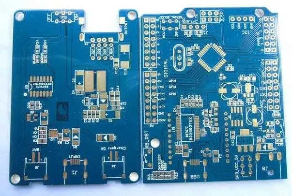
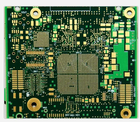
In the fast-evolving world of video processing applications, the demand for high-performance, compact, and reliable printed circuit boards (PCBs) is higher than ever. Whether it's for streaming devices, video cameras, or real-time video analytics systems, advanced PCB manufacturing techniques play a critical role in meeting the stringent requirements of these technologies. This blog dives deep into cutting-edge methods such as HDI PCB for video processing, microvia PCB video designs, blind via PCB video layouts, buried via PCB video structures, and sequential lamination in video PCB production. We'll explore how these techniques enhance signal integrity, reduce latency, and support high-density designs for video processing needs.
Why Advanced PCB Techniques Matter for Video Processing
Video processing applications require PCBs that can handle high-speed data transfer, maintain signal clarity, and fit into increasingly smaller devices. Traditional PCB designs often fall short in meeting these demands due to limitations in layer count, trace width, and signal interference. Advanced manufacturing techniques address these challenges by enabling denser routing, minimizing signal loss, and supporting high-frequency signals—crucial for video processing tasks like 4K/8K streaming or real-time rendering. Let’s break down the key techniques that make this possible.
What is HDI PCB for Video Processing?
High-Density Interconnect (HDI) PCB technology is a game-changer for video processing applications. HDI PCBs are designed with finer traces, smaller vias, and tighter spacing, allowing for more components to be packed into a smaller area. This is especially important for compact devices like video cameras or portable streaming gadgets where space is limited but performance cannot be compromised.
In video processing, HDI PCBs excel by supporting high-speed signals with minimal crosstalk and interference. For instance, they can handle data rates exceeding 10 Gbps, which is essential for transmitting uncompressed 4K video signals. Additionally, HDI designs reduce the number of layers needed compared to traditional boards, cutting down on manufacturing costs while maintaining performance.
The benefits of HDI PCB for video processing include:
- Enhanced signal integrity for high-frequency video signals.
- Reduced board size, ideal for compact video devices.
- Lower power consumption due to shorter signal paths.
Microvia PCB Video Designs: Precision at a Micro Scale
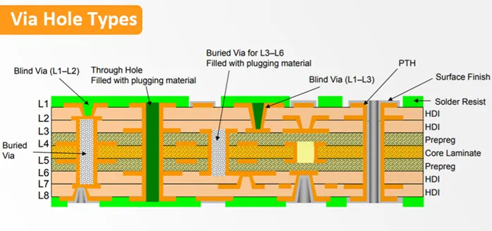
Microvias are tiny holes, often less than 0.15 mm in diameter, used to connect layers in a PCB. In microvia PCB video applications, these small vias enable higher density and more efficient routing of signals. Unlike traditional through-hole vias that pass through the entire board, microvias connect only specific layers, saving space and reducing signal path length.
For video processing, microvias are critical in maintaining signal integrity at high frequencies. Shorter signal paths mean less latency and reduced risk of signal degradation—key factors when dealing with real-time video data. For example, a microvia PCB video design can achieve impedance control within ±10% tolerance, ensuring stable performance for high-speed signals like HDMI or DisplayPort interfaces.
Key advantages of microvia PCB video designs include:
- Higher component density for complex video processing circuits.
- Improved thermal management due to thinner layers.
- Better reliability for high-frequency video signals.
Blind Via PCB Video Layouts: Optimizing Space and Performance
Blind vias are another advanced technique used in PCB manufacturing for video processing. These vias start on an outer layer of the PCB but do not pass through the entire board, terminating at an inner layer. In blind via PCB video designs, this approach saves space on the opposite side of the board, allowing for more components or additional routing.
In video processing applications, blind vias help reduce signal interference by shortening the path signals must travel. This is particularly useful in multilayer boards where high-speed video signals, such as those at 5 GHz or higher, need to avoid crosstalk. Blind vias also improve the board’s mechanical strength by reducing the number of full through-holes, which can weaken the structure.
Benefits of blind via PCB video layouts include:
- Increased design flexibility for compact video devices.
- Reduced signal loss for high-speed video transmission.
- Enhanced board durability for rugged video processing equipment.
Buried Via PCB Video Structures: Hidden Connections for Efficiency
Buried vias are connections that exist entirely within the inner layers of a PCB, invisible from the outer surfaces. In buried via PCB video structures, these vias free up space on the outer layers for additional components or traces, which is invaluable for densely packed video processing boards.
For video applications, buried vias are often used in conjunction with HDI technology to create complex multilayer designs. They help manage high-speed signals by isolating critical connections within inner layers, reducing electromagnetic interference (EMI). This is especially important for video processing systems handling multiple data streams simultaneously, where signal clarity is paramount.
Advantages of buried via PCB video structures include:
- Maximized surface area for component placement in video devices.
- Reduced EMI for cleaner video signal transmission.
- Support for high-layer-count boards in advanced video systems.
Sequential Lamination in Video PCB Production: Building Complexity Layer by Layer
Sequential lamination is a manufacturing process used to create multilayer PCBs by laminating layers in stages rather than all at once. In sequential lamination video PCB production, this technique allows for the integration of advanced via types like microvias, blind vias, and buried vias at different stages of the build. The result is a highly customized board tailored to the specific needs of video processing applications.
This method is particularly beneficial for video processing PCBs because it supports the creation of high-density designs with precise impedance control. For instance, sequential lamination can achieve layer-to-layer registration accuracy within 0.05 mm, ensuring reliable connections for high-speed video signals. It also enables the use of different materials in various layers, optimizing thermal and electrical performance for video systems.
Key benefits of sequential lamination in video PCB production include:
- Ability to build complex, high-density video processing boards.
- Precise control over signal paths for minimal latency.
- Flexibility to incorporate mixed materials for enhanced performance.
How These Techniques Enhance Video Processing Applications
Each of these advanced PCB manufacturing techniques contributes uniquely to the performance of video processing applications. Let’s look at how they work together to address common challenges:
- High-Speed Data Transfer: HDI PCBs, microvias, and blind/buried vias reduce signal path lengths, enabling data rates above 10 Gbps for seamless 4K/8K video streaming.
- Compact Design: By increasing component density and optimizing space, these methods allow for smaller, lighter video devices without sacrificing functionality.
- Signal Integrity: Tight impedance control and reduced EMI ensure that video signals remain clear and free from distortion, even at high frequencies like 6 GHz.
- Reliability: Advanced techniques like sequential lamination improve the structural integrity of PCBs, making them suitable for demanding video processing environments.
For example, a video processing board for a professional camera might use an HDI design with microvias and buried vias to handle multiple high-speed inputs while fitting into a handheld device. The use of sequential lamination ensures that each layer is optimized for thermal dissipation, preventing overheating during extended use.
Choosing the Right Technique for Your Video Processing Needs
Selecting the appropriate PCB manufacturing technique depends on the specific requirements of your video processing application. Here are some considerations to guide your decision:
- For ultra-compact devices like wearable cameras, prioritize HDI PCB for video processing with microvias to maximize space efficiency.
- For multilayer boards with complex routing, such as video analytics hardware, opt for blind via PCB video layouts and buried via structures to manage high-density connections.
- For custom designs requiring precise impedance matching, sequential lamination in video PCB production offers the flexibility to fine-tune each layer.
Working with a trusted PCB manufacturer can help you navigate these choices, ensuring that your board meets the performance and cost requirements of your project.
Future Trends in PCB Manufacturing for Video Processing
As video processing technology continues to advance, so too will PCB manufacturing techniques. Emerging trends include the use of even smaller microvias (below 0.1 mm), the integration of flexible materials in HDI designs, and the adoption of automated manufacturing processes for sequential lamination. These innovations promise to further enhance the performance of video processing systems, supporting applications like virtual reality, augmented reality, and real-time AI-driven video analysis.
Additionally, the push for sustainability in electronics manufacturing is leading to the development of eco-friendly materials and processes for advanced PCBs. This means that future video processing boards will not only be faster and smaller but also more environmentally responsible.
Conclusion: Elevating Video Processing with Advanced PCB Techniques
The landscape of video processing applications is defined by the need for speed, compactness, and reliability. Advanced PCB manufacturing techniques like HDI PCB for video processing, microvia PCB video designs, blind via PCB video layouts, buried via PCB video structures, and sequential lamination in video PCB production are essential tools in meeting these demands. By leveraging these methods, engineers can create cutting-edge video processing systems that deliver exceptional performance in even the most challenging environments.
Understanding and applying these techniques ensures that your video processing projects stay ahead of the curve, whether you’re designing for consumer electronics, professional equipment, or industrial applications. With the right approach, the possibilities for innovation in video technology are limitless.


