 ALLPCB


In the fast-evolving world of automotive technology, Advanced Driver Assistance Systems (ADAS) are transforming how we drive, making vehicles safer and smarter. A key component of ADAS is the automotive radar system, which relies heavily on well-designed printed circuit boards (PCBs) to ensure accurate performance. If you're an engineer or designer looking for ADAS PCB layout guidelines, you're in the right place. This blog will provide actionable tips and best practices for radar PCB design, focusing on critical aspects like antenna placement, minimizing interference in radar systems, and high-frequency PCB layout techniques.
Whether you're working on a new radar module or optimizing an existing design, following these guidelines can help you achieve reliable signal integrity and performance in high-frequency environments. Let's dive into the details of crafting effective PCB layouts for automotive radar systems.
Why ADAS PCB Layout Matters for Automotive Radar Systems
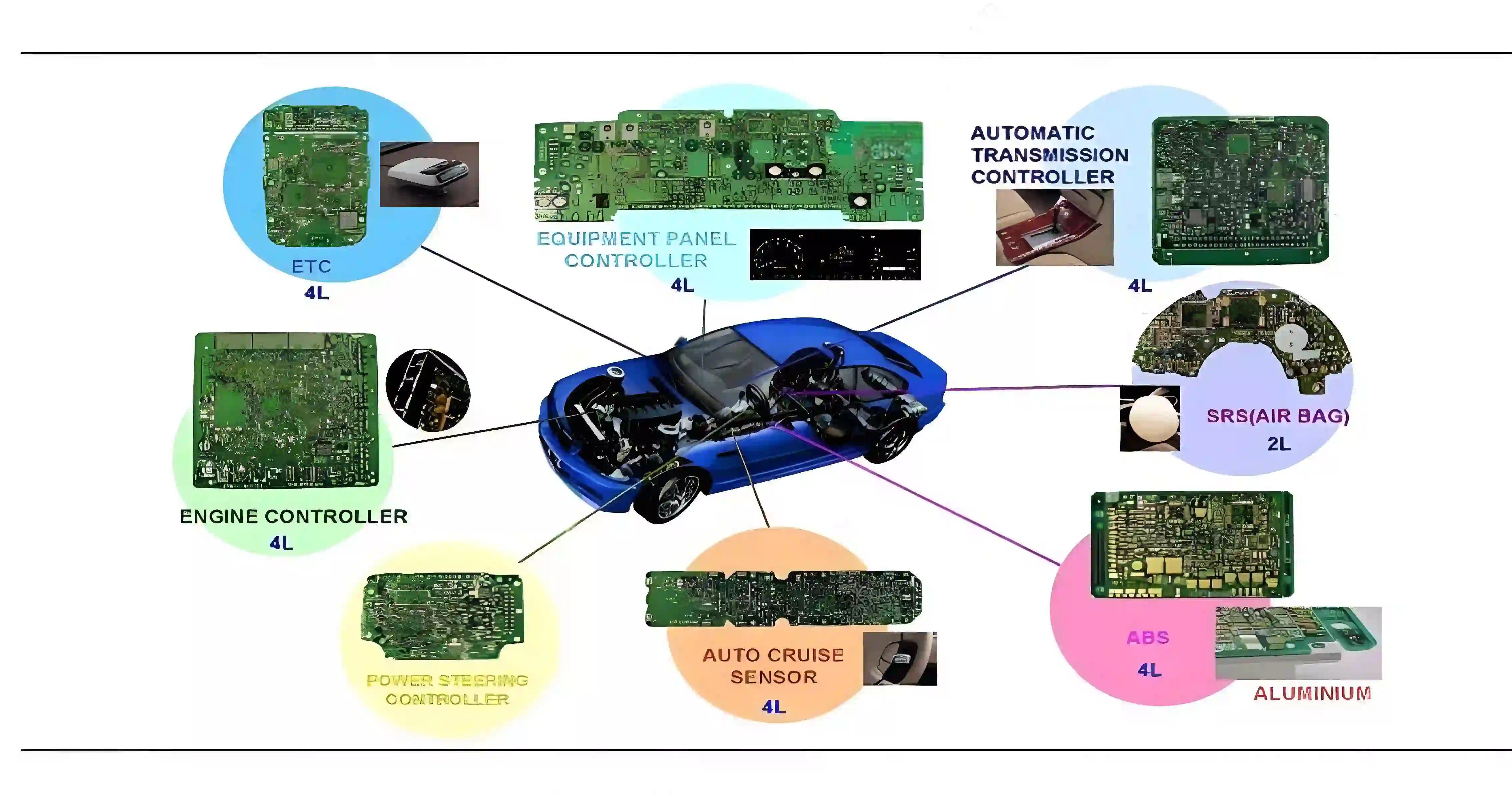
Automotive radar systems are the backbone of many ADAS features, such as adaptive cruise control, blind-spot detection, and collision avoidance. These systems operate at high frequencies, often in the 24 GHz to 79 GHz range, to detect objects with precision. A poorly designed PCB can lead to signal loss, interference, or inaccurate readings, which could compromise safety.
A well-executed ADAS PCB layout ensures that radar signals are transmitted and received with minimal distortion. It also helps manage heat, reduces electromagnetic interference (EMI), and supports the compact designs required in modern vehicles. With the right approach to radar PCB design, you can enhance system reliability and meet strict automotive standards.
Key Principles of Radar PCB Design for ADAS
Designing a PCB for automotive radar systems requires attention to several critical factors. Below are the core principles to keep in mind when working on high-frequency PCB layout for ADAS applications.
1. Material Selection for High-Frequency Performance
The choice of PCB material is crucial for radar systems operating at high frequencies. Standard FR-4 materials may not suffice due to their higher dielectric losses at frequencies above 10 GHz. Instead, opt for specialized high-frequency laminates like Rogers RO4000 series or PTFE-based materials. These materials offer low dielectric constants (typically between 2.2 and 3.5) and low loss tangents (around 0.002 to 0.004), ensuring minimal signal attenuation.
Using the right material helps maintain signal integrity, especially for radar signals in the 77-79 GHz range used in long-range automotive applications. Additionally, ensure that the material's thermal properties can handle the heat generated by high-frequency components.
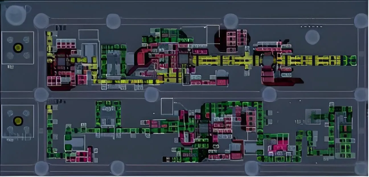
2. Layer Stackup for Signal Integrity
A proper layer stackup is essential for minimizing interference in radar systems. Most radar PCBs use a multi-layer design to separate high-frequency signals from power and ground planes. A typical stackup might include:
- Top Layer: RF components and antenna structures.
- Inner Layer 1: Ground plane for shielding.
- Inner Layer 2: Power distribution.
- Bottom Layer: Additional routing or ground.
Keep signal traces on the top layer short to reduce parasitic effects. Place a continuous ground plane directly beneath the signal layer to provide a low-impedance return path, which is vital for frequencies above 24 GHz. This setup also helps in reducing EMI, a common issue in high-frequency designs.
Antenna Placement in Radar PCB Design
One of the most critical aspects of radar PCB design is antenna placement. Antennas in automotive radar systems are responsible for transmitting and receiving high-frequency signals, and their positioning directly impacts system accuracy.
3. Positioning for Optimal Signal Coverage
Place antennas at the edge of the PCB or on a dedicated layer to avoid interference from other components. For patch antennas commonly used in radar systems, ensure they are oriented to cover the desired field of view (FOV). For example, a forward-looking radar might require antennas aligned at a 0-degree angle, while side-looking systems might need a 90-degree orientation.
Maintain a clear area around the antenna, free from tall components or metal structures, to prevent signal blockage. A clearance of at least 5 mm around the antenna is often recommended, though this can vary based on the specific frequency and design requirements.
4. Isolation from Other Components
To avoid coupling effects, isolate antennas from high-speed digital circuits and power supplies. Use ground planes or shielding vias around the antenna area to create a barrier against stray signals. This practice is especially important in compact designs where space is limited, as it helps in minimizing interference in radar systems.
Minimizing Interference in Radar Systems
Interference is a major challenge in automotive radar systems due to the presence of multiple electronic systems in a vehicle. A well-thought-out ADAS PCB layout can significantly reduce noise and ensure accurate radar performance.
5. Grounding Techniques
Effective grounding is key to minimizing interference in radar systems. Use a solid ground plane beneath RF traces to provide a consistent return path for signals. Avoid splitting the ground plane, as this can create loops that act as antennas for EMI.
Additionally, place stitching vias around the edges of the PCB and near high-frequency components. These vias connect multiple ground layers, reducing the risk of ground bounce and ensuring a low-impedance path. For a 77 GHz radar system, spacing vias at intervals of λ/20 (where λ is the wavelength, approximately 3.9 mm at 77 GHz) can effectively suppress unwanted resonances.
6. Trace Routing and Impedance Matching
In high-frequency PCB layout, trace routing must be precise to maintain signal integrity. Use controlled impedance traces, typically designed for 50 ohms, to match the impedance of RF components and antennas. Tools like microstrip or coplanar waveguide calculators can help determine the correct trace width and spacing based on the PCB material and frequency.
Keep RF traces as short and straight as possible to minimize signal loss. Avoid sharp corners; instead, use 45-degree bends or curved traces to reduce reflections. For example, a trace carrying a 77 GHz signal should ideally be shorter than 10 mm to limit attenuation to less than 0.5 dB.
Thermal Management in ADAS PCB Layout
High-frequency radar systems generate significant heat, especially in compact automotive designs. Poor thermal management can degrade component performance and reduce the lifespan of the PCB.
7. Heat Dissipation Strategies
Place heat-generating components like power amplifiers away from sensitive RF circuits. Use thermal vias to transfer heat from the top layer to a dedicated heat sink or the bottom layer. For instance, a grid of thermal vias with a diameter of 0.3 mm and spacing of 1.2 mm can effectively dissipate heat from a high-power RF chip.
Consider adding copper pours connected to ground on unused areas of the PCB to act as heat spreaders. This technique helps distribute heat evenly and prevents hot spots that could affect radar accuracy.
Design Tools and Simulation for Radar PCB Layout
Modern radar PCB design relies heavily on simulation tools to predict performance before fabrication. Use electromagnetic (EM) simulation software to analyze signal integrity, antenna radiation patterns, and EMI risks. These tools can help you fine-tune antenna placement and trace routing for optimal results.
Additionally, perform pre-layout simulations to verify impedance matching and post-layout checks to identify potential interference sources. For high-frequency designs, even a small mismatch can lead to significant signal loss, so simulation is a critical step in the high-frequency PCB layout process.
Compliance with Automotive Standards
Automotive radar systems must adhere to strict industry standards to ensure safety and reliability. When designing an ADAS PCB layout, consider requirements from organizations like the International Organization for Standardization (ISO) and the Society of Automotive Engineers (SAE). Key standards include ISO 26262 for functional safety and AEC-Q100 for component reliability under harsh conditions.
Ensure that your design can withstand temperature extremes (typically -40°C to 85°C), vibrations, and humidity, as these are common in automotive environments. Use components rated for automotive applications and conduct thorough testing to validate performance.
Conclusion: Building Reliable Radar Systems with ADAS PCB Layout
Creating an effective ADAS PCB layout for automotive radar systems is a complex but rewarding task. By focusing on material selection, proper antenna placement, minimizing interference in radar systems, and robust high-frequency PCB layout techniques, you can design PCBs that deliver accurate and reliable performance. These guidelines are tailored to help engineers navigate the challenges of radar PCB design, ensuring that ADAS features function seamlessly in real-world conditions.
Remember to leverage simulation tools, prioritize thermal management, and adhere to automotive standards throughout the design process. With careful planning and attention to detail, your radar PCB can contribute to safer, smarter vehicles. At ALLPCB, we're committed to supporting your design journey with high-quality manufacturing solutions tailored to automotive applications.


