ALLPCB


In the fast-paced world of electronics, achieving optimal signal integrity is a cornerstone of successful PCB design. If you're wondering how to ensure clean, reliable signals in your printed circuit board (PCB), the answer lies in a well-thought-out PCB stackup design. A proper stackup not only enhances signal integrity but also minimizes crosstalk and maintains impedance control. In this comprehensive guide, we'll explore the essentials of PCB stackup design, focusing on signal layer placement, minimizing crosstalk, and impedance control for PCB projects. Whether you're a seasoned engineer or just starting out, this deep dive will equip you with actionable insights to elevate your designs.
What is PCB Stackup Design and Why Does It Matter for Signal Integrity?
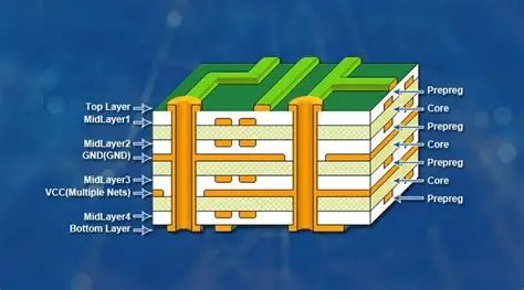
PCB stackup design refers to the arrangement of conductive and insulating layers in a printed circuit board. These layers include signal layers (for routing traces), power planes, and ground planes, stacked in a specific order to meet electrical and mechanical requirements. The way these layers are organized directly impacts signal integrity, which is the ability of a signal to travel from source to destination without distortion or interference.
A well-designed stackup ensures that high-speed signals maintain their quality, reduces electromagnetic interference (EMI), and prevents issues like crosstalk. For instance, in high-speed designs operating at frequencies above 100 MHz, even a small mismatch in impedance can cause signal reflections, leading to data errors. By prioritizing PCB stackup signal integrity, you can avoid costly redesigns and ensure your board performs reliably in real-world applications.
Key Benefits of a Proper PCB Stackup
- Enhanced Signal Integrity: Reduces noise and signal distortion for clearer data transmission.
- Minimized Crosstalk: Prevents interference between adjacent traces, especially in dense designs.
- Impedance Control: Maintains consistent impedance for high-speed signals, avoiding reflections.
- Improved EMI Performance: Reduces radiated emissions through proper grounding and layer arrangement.

The Basics of Signal Layer Placement in PCB Stackup Design
Signal layer placement is a critical aspect of PCB stackup design. The position of signal layers relative to power and ground planes determines how well signals are shielded from noise and interference. In multi-layer boards (4 layers or more), signal layers are typically sandwiched between ground or power planes to create a controlled environment for signal transmission.
Guidelines for Effective Signal Layer Placement
- Place High-Speed Signals Close to Ground Planes: Positioning high-speed signal layers adjacent to a ground plane minimizes loop inductance and provides a return path for currents. This reduces noise and improves signal integrity. For example, in a 6-layer board, place critical signal traces on layers 2 and 5, with ground planes on layers 1, 3, 4, and 6.
- Separate Analog and Digital Signals: Keep analog and digital signal layers apart to prevent interference. If possible, dedicate separate layers or sections of the board to each type of signal.
- Avoid Signal Layers on Outer Surfaces: Exposing signal traces on the top or bottom layers increases the risk of EMI. Use inner layers for routing critical signals whenever possible.
By following these principles, you can ensure that your signal layer placement supports robust signal integrity and reduces the chances of performance issues in high-speed designs.
Minimizing Crosstalk in PCB Stackup Design
Crosstalk occurs when a signal on one trace interferes with a signal on an adjacent trace, leading to noise and potential data corruption. In high-density PCB designs, where traces are closely packed, minimizing crosstalk is essential for maintaining signal integrity. A well-planned stackup can significantly reduce this interference.
Strategies for Minimizing Crosstalk
- Use Ground Planes as Shields: Place ground planes between signal layers to act as a barrier against crosstalk. For instance, in an 8-layer PCB stackup, alternate signal and ground layers to isolate traces carrying high-speed signals.
- Increase Trace Spacing: Follow the 3W rule, which suggests maintaining a spacing of at least three times the trace width between adjacent high-speed traces. For a 5-mil trace, this means a spacing of 15 mils to reduce coupling effects.
- Route Signals on Different Layers: If spacing is limited, route high-speed signals on different layers to avoid parallel runs over long distances. This reduces the chance of electromagnetic coupling.
- Keep Signal Layers Symmetrical: A symmetrical stackup ensures balanced capacitance and inductance, further reducing crosstalk. For example, in a 4-layer board, use a stackup of Signal-Ground-Power-Signal for symmetry.
Implementing these strategies in your PCB stackup design can drastically cut down on crosstalk, ensuring cleaner signals even in compact, high-speed boards.

Impedance Control in PCB Stackup Design
Impedance control is a cornerstone of high-speed PCB design. Characteristic impedance, measured in ohms, determines how a signal propagates along a trace. If the impedance of a trace doesn’t match the source or load (e.g., 50 ohms for many high-speed standards), reflections occur, degrading signal quality. A well-designed stackup is key to achieving consistent impedance control for PCB traces.
How to Achieve Impedance Control
- Define Layer Thickness and Materials: The dielectric constant (Dk) of the insulating material and the thickness between signal layers and reference planes affect impedance. For example, using a material with a Dk of 4.2 (common for FR-4) and a dielectric thickness of 10 mils can help achieve a 50-ohm impedance for a 5-mil wide trace.
- Use Reference Planes: Ensure signal layers are adjacent to a continuous ground or power plane. This creates a controlled impedance environment, as the plane acts as a reference for the signal return path.
- Calculate Trace Widths: Use impedance calculators or simulation tools to determine the correct trace width for your target impedance. For a 50-ohm single-ended trace on a standard 4-layer PCB board, a width of around 6-8 mils is often suitable, depending on the dielectric thickness.
- Maintain Uniform Stackup Symmetry: An asymmetrical stackup can lead to uneven impedance across layers. Balance the stackup to keep impedance consistent throughout the board.
By focusing on impedance control in your PCB stackup design, you can prevent signal reflections and ensure reliable performance, especially in applications like USB, HDMI, or DDR memory interfaces operating at speeds above 1 GHz.
Common PCB Stackup Configurations for Signal Integrity
Different projects call for different stackup configurations, depending on the number of layers and design requirements. Below are some common stackups used to optimize PCB stackup signal integrity.
4-Layer Stackup
A 4-layer board is a cost-effective choice for many designs. A typical configuration is:
- Layer 1: Signal (Top)
- Layer 2: Ground
- Layer 3: Power
- Layer 4: Signal (Bottom)
This setup provides good shielding for inner traces and supports basic impedance control, though it may not suffice for very high-speed designs due to limited layer count.
6-Layer Stackup
For more complex designs, a 6-layer stackup offers additional flexibility:
- Layer 1: Ground
- Layer 2: Signal
- Layer 3: Ground
- Layer 4: Power
- Layer 5: Signal
- Layer 6: Ground
This configuration isolates high-speed signals with multiple ground planes, improving signal integrity and reducing crosstalk.
8-Layer Stackup
For high-speed, high-density designs, an 8-layer stackup is ideal:
- Layer 1: Ground
- Layer 2: Signal
- Layer 3: Ground
- Layer 4: Power
- Layer 5: Power
- Layer 6: Ground
- Layer 7: Signal
- Layer 8: Ground
This setup provides excellent shielding, multiple power distribution layers, and ample space for routing complex signals.
Best Practices for Designing a PCB Stackup
Creating a PCB stackup that prioritizes signal integrity requires careful planning and attention to detail. Here are some best practices to follow:
- Collaborate with Your Manufacturer Early: Discuss stackup options and material choices with your PCB fabricator to ensure manufacturability and cost-effectiveness.
- Use Simulation Tools: Leverage software tools to simulate signal integrity, impedance, and crosstalk before finalizing your stackup. This helps identify potential issues early.
- Prioritize Symmetry: A symmetrical stackup prevents warping during manufacturing and maintains uniform electrical properties across layers.
- Plan for Thermal Management: Ensure power and ground planes are thick enough to handle current loads without overheating, which can affect signal performance.
- Document Your Design: Clearly specify layer assignments, materials, and impedance requirements in your design files to avoid miscommunication during production.
By adhering to these practices, you can create a PCB stackup design that not only meets performance goals but also streamlines the manufacturing process.
Challenges in PCB Stackup Design and How to Overcome Them
While designing a PCB stackup for signal integrity sounds straightforward, several challenges can arise. Here’s how to tackle them:
- Layer Count Limitations: If your design requires more layers than your budget allows, optimize routing on fewer layers by prioritizing critical signals and using wider spacing to reduce crosstalk.
- Material Constraints: High-frequency designs may require specialized materials with lower dielectric constants. Work with your manufacturer to balance performance and cost.
- Complex Routing Needs: In dense designs, routing high-speed signals without violating design rules can be tough. Use automated routing tools and manual adjustments to ensure compliance with impedance and spacing guidelines.
Addressing these challenges proactively will help you achieve a robust PCB stackup design, even under tight constraints.
Conclusion: Mastering PCB Stackup Design for Signal Integrity
Unlocking signal integrity through effective PCB stackup design is a game-changer for any electronics project. By focusing on signal layer placement, minimizing crosstalk, and ensuring impedance control for PCB traces, you can create boards that perform reliably at high speeds and in challenging environments. Remember to prioritize symmetry, use ground planes for shielding, and collaborate with your manufacturer to refine your stackup. With these strategies in hand, you’re well on your way to designing PCBs that meet the demands of modern electronics.
Whether you’re working on a simple 4-layer board or a complex 12-layer design, a thoughtful approach to PCB stackup signal integrity will set your project up for success. Start implementing these principles in your next design, and watch as signal quality and overall performance reach new heights.