 ALLPCB


In the fast-paced world of electronics, high-speed circuits demand precision to ensure signals travel without distortion. Impedance mismatches in printed circuit board (PCB) design can lead to reflections, noise, and data errors, compromising performance. This is where impedance calculators become invaluable tools for engineers. By enabling precise control over trace impedance, these calculators help optimize signal integrity, ensuring reliable operation in high-frequency applications. In this blog, we explore the role of impedance calculators, how they work, and practical strategies for using them to enhance PCB design.
Our goal is to equip engineers with actionable insights to tackle signal integrity challenges. Whether you're designing for 5G, IoT, or automotive systems, understanding impedance calculators can make the difference between a robust design and costly failures.
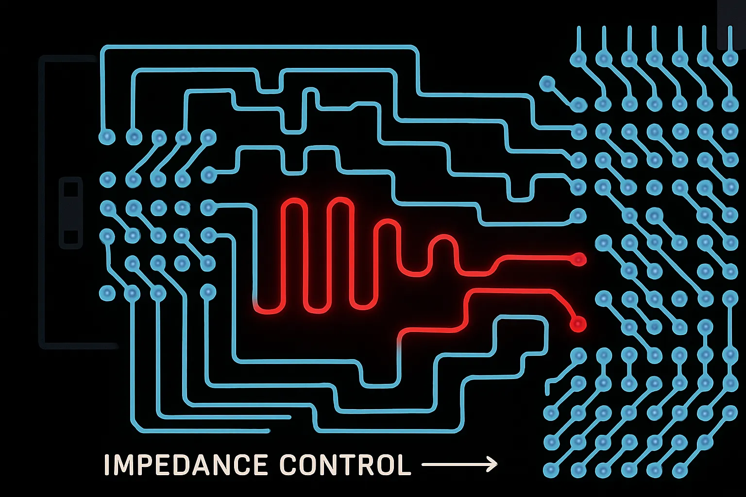
What Is Impedance in PCB Design?
Impedance, measured in ohms (Ω), represents the opposition to alternating current in a circuit, combining resistance, capacitance, and inductance. In PCB design, characteristic impedance refers to the impedance of a transmission line, such as a microstrip or stripline, which carries high-frequency signals. For signals above 50 MHz, maintaining consistent impedance is critical to prevent reflections that degrade signal quality. For example, a typical single-ended trace might target 50 Ω, while differential pairs for USB or HDMI often aim for 90 Ω.
Impedance mismatches occur when the source, trace, and receiver impedances differ, causing part of the signal to reflect back. This can result in distortion, electromagnetic interference EMI compliance testing, and reduced signal-to-noise ratio. Impedance calculators simplify the process of designing traces to match target impedance values, ensuring maximum power transfer and minimal signal degradation.
Why Impedance Calculators Are Essential
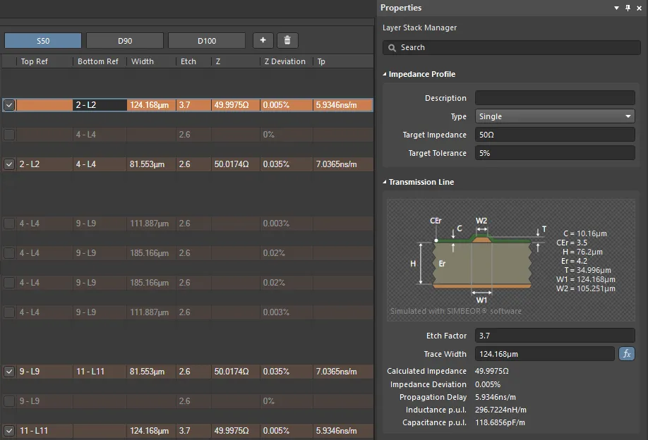
Impedance calculators are specialized tools that compute the characteristic impedance of PCB traces based on physical parameters like trace width, thickness, dielectric constant, and layer stackup. Unlike manual calculations, which rely on complex equations like Wadell's or IPC-2141, these tools provide quick, accurate results, saving time and reducing errors.
Key benefits include:
- Precision: Calculators account for variables like dielectric thickness and copper weight, delivering results within ±10% tolerance, as required by most high-speed standards.
- Efficiency: Engineers can iterate designs rapidly, adjusting parameters to meet target impedance without tedious hand calculations.
- Versatility: Tools support various transmission line types, including microstrip, stripline, and differential pairs, catering to diverse applications.
Without proper impedance control, high-speed signals—such as those in DDR4 memory (up to 3.2 GHz) or PCIe 5.0 (16 GT/s)—risk data corruption. Impedance calculators bridge the gap between theoretical design and real-world performance.
How Impedance Calculators Work
Impedance calculators use mathematical models to determine the characteristic impedance of a transmission line. The most accurate tools employ Wadell's equations, which account for frequency-dependent effects like loss tangent and dispersion. Simpler calculators may use IPC-2141 equations, suitable for low-frequency designs but less precise for high-speed applications.
Key Input Parameters
To calculate impedance, engineers input the following:
- Trace Width (W): Wider traces reduce impedance. For a 50 Ω microstrip, a typical width might be 0.2 mm on a standard FR-4 board.
- Trace Thickness (T): Thinner copper increases impedance. Standard copper thickness is 1 oz/ft² (0.035 mm).
- Dielectric Constant (Dk): The substrate material's Dk affects impedance. FR-4 has a Dk of ~4.3, while low-Dk laminates like Rogers 4350B (~3.5) are used for high-frequency designs.
- Dielectric Thickness (H): The distance between the trace and reference plane. Thicker dielectrics increase impedance.
- Trace Spacing (S): For differential pairs, spacing impacts coupling and impedance. A typical USB differential pair might have 0.15 mm spacing.
Types of Transmission Lines
Calculators support various configurations:
- Microstrip: Surface traces with one reference plane, common for high-speed routing.
- Stripline: Traces embedded between two ground planes, offering better EMI shielding.
- Differential Pairs: Two parallel traces for signals like USB or Ethernet, requiring precise spacing control.
- Coplanar Waveguide: Traces with adjacent ground planes on the same layer, used in RF designs.
By inputting these parameters, the calculator outputs the characteristic impedance, allowing engineers to adjust trace geometry or stackup to meet design requirements.
Factors Affecting Impedance in PCB Design
Several factors influence impedance, and calculators help engineers account for them:
- Substrate Material: The dielectric constant and loss tangent of materials like FR-4 or high-frequency laminates impact signal propagation. For instance, a 10% variation in Dk can shift impedance by 5 Ω.
- Trace Geometry: Small changes in width or thickness—due to manufacturing tolerances (±20% for standard processes)—can alter impedance significantly.
- Layer Stackup: The arrangement of signal, power, and ground layers affects impedance and crosstalk. A well-designed stackup ensures consistent reference planes for return paths.
- Frequency: At higher frequencies (>1 GHz), skin effect and dielectric losses become pronounced, requiring precise impedance control.
- Solder Mask: Its thickness and dielectric constant can lower impedance slightly, often by 1-2 Ω.
Understanding these factors allows engineers to use calculators effectively, ensuring designs meet stringent signal integrity requirements.
Practical Tips for Using Impedance Calculators
To optimize signal integrity issues, follow these best practices when using impedance calculators:
- Define Target Impedance Early: Consult component datasheets to determine required impedance. For example, SDIO signals typically need 50 Ω single-ended traces, while HDMI requires 100 Ω differential pairs.
- Select Appropriate Materials: Choose substrates with stable Dk values. For high-speed designs, consider low-Dk materials to reduce signal loss.
- Verify Stackup: Work with your PCB manufacturer to define a stackup that supports controlled impedance. A 4-layer board with 0.2 mm dielectric thickness is common for 50 Ω microstrips.
- Account for Tolerances: Design with manufacturing tolerances in mind. If a calculator suggests a 0.2 mm trace width, ensure the fabricator can maintain ±20% accuracy.
- Simulate and Validate: Use tools like SPICE or field solvers to simulate impedance and verify calculator results. Post-layout analysis with tools like Altium Designer or OrCAD can catch discrepancies.
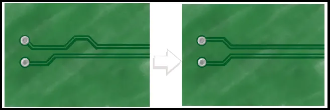
- Minimize Vias and Stubs: Vias introduce impedance discontinuities. Use blind or micro vias for high-speed signals to reduce stubs, which can cause reflections.
By integrating these practices, engineers can leverage impedance calculators to achieve robust, high-performance PCB designs.
Common Signal Integrity Challenges and Solutions
Even with impedance calculators, signal integrity issues can arise. Here are common challenges and how to address them:
- Reflections: Caused by impedance mismatches, reflections distort signals. Solution: Use termination resistors (e.g., 50 Ω series termination) to absorb signal energy.
- Crosstalk: Adjacent traces can couple unwanted signals. Solution: Increase trace spacing (e.g., 3x trace width) and use ground planes for shielding.
- EMI: Impedance discontinuities can radiate noise. Solution: Ensure continuous reference planes and avoid gaps in ground layers.
- Power Integrity: Voltage fluctuations affect signal quality. Solution: Place decoupling capacitors (e.g., 0.1 µF) near IC power pins to stabilize the power delivery network (PDN).
Impedance calculators help mitigate these issues by ensuring traces are designed to minimize reflections and maintain consistent impedance.
Advanced Tools for Impedance Control
While online calculators like JLCPCB's or Altium's are user-friendly, advanced PCB design software offers integrated impedance analysis:
- Altium Designer: Features a built-in impedance profiler for real-time calculations, supporting complex stackups and differential pairs.
- Cadence OrCAD: Provides SPICE-based simulations and harmonic balance analysis to model nonlinear effects.
- Zuken PI Simulator: Validates PDN impedance against IC vendor specifications, reducing over-engineering.
- Hyperlynx: Industry-standard for signal integrity analysis, offering eye diagram and TDR simulations.
These tools complement calculators by providing deeper insights into impedance behavior, especially for high-speed designs operating at 10 Gbps or higher.
How ALLPCB Supports Impedance-Controlled PCB Design
For engineers tackling high-speed PCB designs, partnering with a reliable manufacturer is crucial. ALLPCB's advanced manufacturing capabilities ensure precise impedance control, with tolerances as tight as ±10% for critical traces. Our quick-turn prototyping allows designers to test and iterate impedance-controlled designs rapidly, while global logistics ensure timely delivery. By leveraging state-of-the-art equipment and rigorous quality checks, we help engineers translate impedance calculations into high-performance boards, supporting applications from IoT to automotive electronics.
Conclusion: Mastering Signal Integrity with Impedance Calculators
Impedance calculators are indispensable for modern PCB design, enabling engineers to achieve precise control over signal integrity. By understanding how to use these tools and applying best practices—like selecting appropriate materials, verifying stackups, and simulating designs—designers can minimize reflections, crosstalk, and EMI. As signal speeds continue to rise, mastering impedance control will remain a cornerstone of reliable electronics.
We encourage engineers to experiment with impedance calculators and collaborate with manufacturers to refine their designs. With the right tools and strategies, you can ensure your PCBs perform flawlessly in even the most demanding applications.


