 ALLPCB


In the fast-paced world of electronics manufacturing, soldering is the backbone of reliable printed circuit board (PCB) assembly. Two dominant techniques—reflow soldering and wave soldering—play critical roles in attaching components to PCBs, each with distinct processes, advantages, and applications. For engineers, selecting the right method can significantly impact production efficiency, cost, and product quality. In this comprehensive guide, we explore the differences between reflow and wave soldering, their ideal use cases, and key considerations to help you make informed decisions for your PCB assembly projects.
Whether you're designing compact, high-density boards or assembling large-scale through-hole components, understanding these soldering methods is essential. Let's dive into the technical details, compare their strengths, and provide practical insights to optimize your manufacturing process.
What is Reflow Soldering?
Reflow soldering is the go-to method for surface-mount technology (SMT) components, widely used in modern electronics due to its precision and adaptability. The process involves applying solder paste—a mixture of powdered solder alloy and flux—onto PCB pads, placing components, and heating the assembly in a controlled reflow oven to melt the solder and form permanent joints.
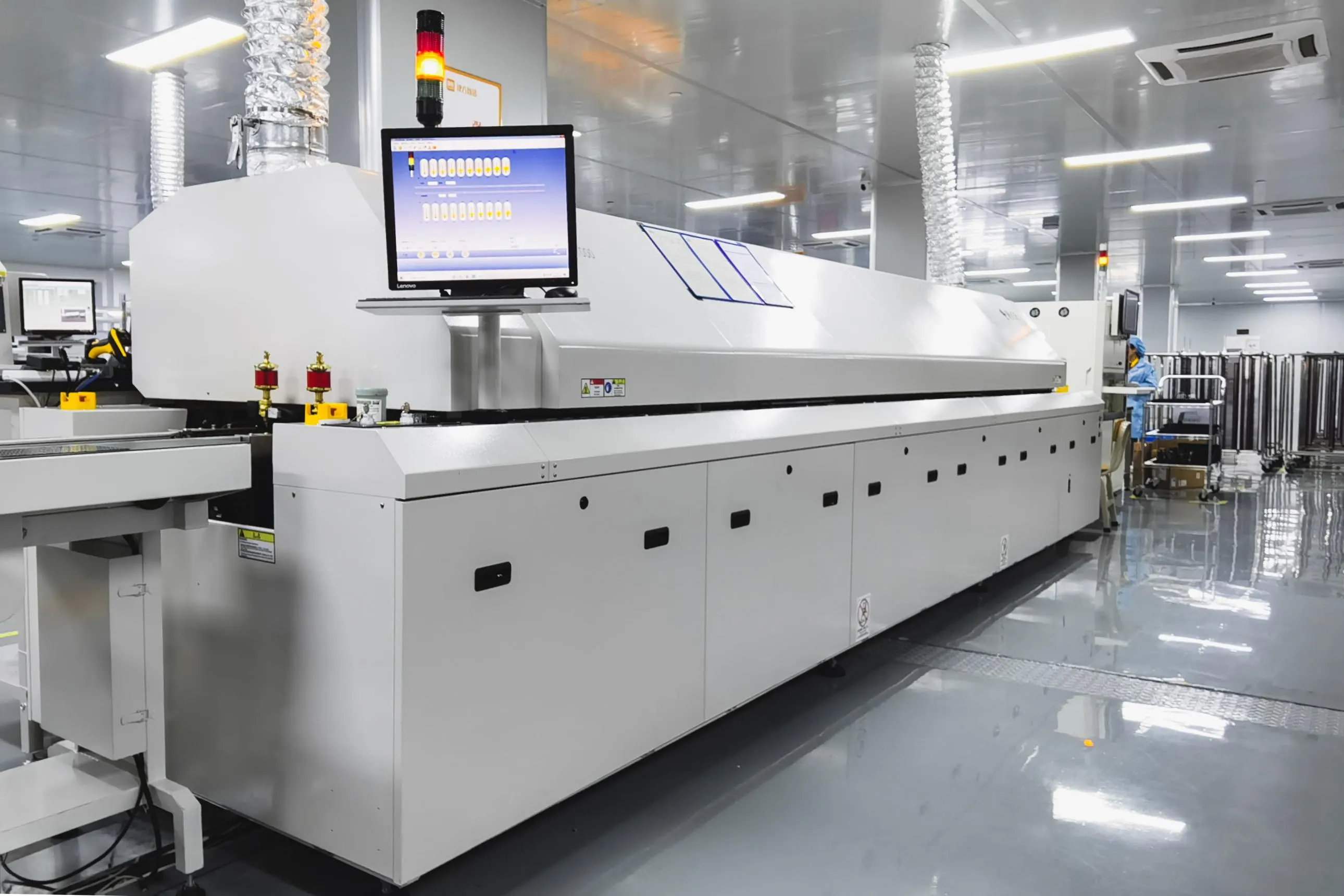
The Reflow Soldering Process
1. Solder Paste Application: Solder paste is deposited onto PCB pads using a stencil printer for precise placement. The paste, typically containing tin, silver, and copper, acts as both an adhesive and a soldering medium.
2. Component Placement: Automated pick-and-place machines position SMT components onto the solder paste-covered pads. The sticky paste holds components in place.
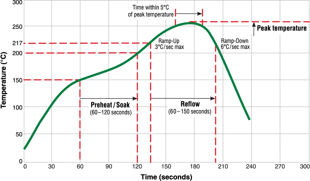
3. Preheating: The PCB enters a reflow oven, where it is gradually heated (2-4°C per second) to 150-180°C to activate the flux, remove oxides, and prevent thermal shock.
4. Thermal Soak: The assembly is held at a steady temperature (around 180-200°C) to ensure even heating and flux activation.
5. Reflow: The temperature ramps up to 220-260°C, melting the solder paste to form liquid joints that bond components to pads.
6. Cooling: The PCB cools at a controlled rate (typically 30-100°C) to solidify solder joints, minimizing thermal stress and ensuring mechanical strength.
Advantages of Reflow Soldering
- Precision: Ideal for fine-pitch components (e.g., 0.5 mm pitch QFPs) and high-density PCBs.
- Automation: Highly automated, reducing labor costs and improving consistency.
- Flexibility: Suitable for single- and double-sided SMT assemblies.
- Reduced Thermal Shock: Controlled heating minimizes stress on components compared to wave soldering.
Limitations
- Equipment Cost: Reflow ovens and stencil printers require significant investment.
- Not Ideal for Through-Hole: Less effective for through-hole components unless using pin-in-paste techniques.
What is Wave Soldering?
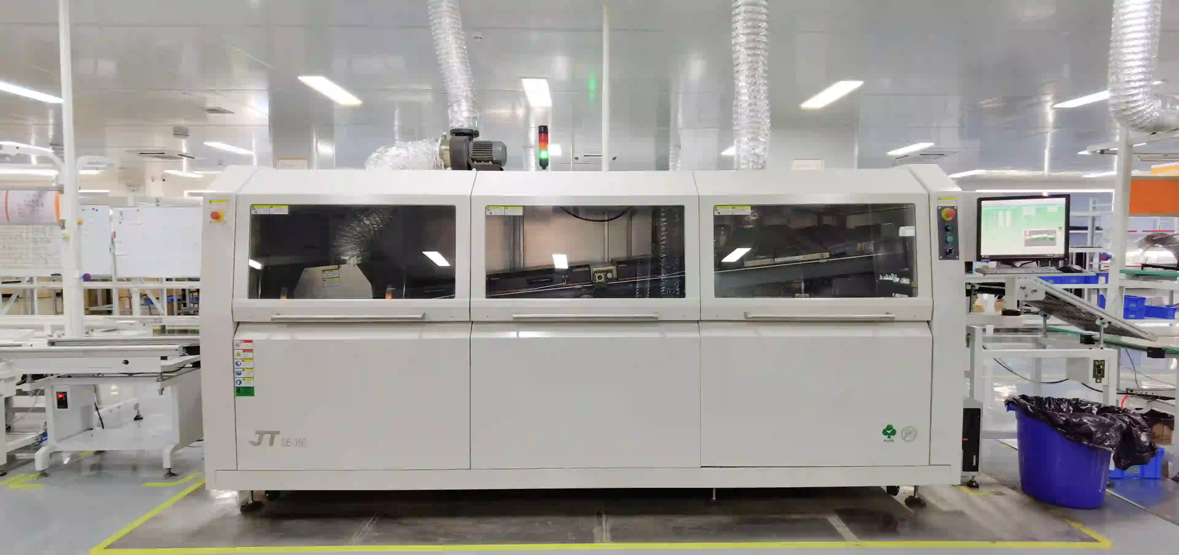
Wave soldering is a bulk soldering process primarily used for through-hole technology (THT) components and some surface-mount assemblies. It involves passing a PCB over a molten solder wave, which creates reliable electrical and mechanical connections in a short time.
The Wave Soldering Process
1. Flux Application: Flux is sprayed onto the PCB's underside to clean component leads and pads, removing oxides for better solder wetting.
2. Preheating: The PCB is preheated to 100-150°C to activate flux and prevent thermal shock when contacting molten solder.
3. Wave Soldering: The PCB passes over a pumped wave of molten solder (typically at 250-260°C), which contacts component leads and pads to form solder joints. Contact time is brief, lasting 2-4 seconds.
4. Cooling: The PCB is cooled using air or water to solidify solder joints and fix components in place.
Advantages of Wave Soldering
- Speed: Efficient for high-volume THT assemblies, soldering multiple boards in seconds.
- Cost-Effective for THT: Lower setup costs for through-hole components compared to reflow for SMT.
- Strong Joints: Produces robust mechanical connections, ideal for components under physical stress (e.g., connectors).
Limitations
- Thermal Stress: High solder temperatures (up to 260°C) can stress sensitive components, risking warpage or cracking.
- Not Suited for Fine-Pitch SMT: Less precise for high-density surface-mount designs.
- Complex Setup: Requires careful control of wave height, conveyor speed, and temperature to avoid defects like bridging or incomplete joints.
Key Differences Between Reflow and Wave Soldering
To choose the right soldering method, engineers must understand how reflow and wave soldering differ in process, application, and performance. Below is a detailed comparison:
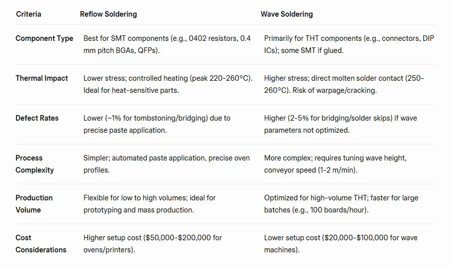
1. Component Type
- Reflow Soldering: Best for SMT components, such as chip resistors, capacitors, and ICs with fine-pitch leads (e.g., 0.4 mm pitch BGAs). It excels in high-density designs where precision is critical.
- Wave Soldering: Primarily used for THT components, like connectors, capacitors, and DIP ICs, where leads pass through PCB holes. It can also solder SMT components if glued to the board's underside, though this is less common.
2. Process Complexity
- Reflow Soldering: Simpler to control due to automated solder paste application and precise oven temperature profiles. Defects like bridging are minimized by accurate paste deposition.
- Wave Soldering: More complex, requiring expertise to adjust wave height, conveyor speed (typically 1-2 m/min), and solder temperature. Improper settings can lead to defects like solder bridges or incomplete joints.
Suggested Reading: Wave Soldering vs. Reflow for Double-Sided Boards: Choosing the Right Process
3. Thermal Impact
- Reflow Soldering: Lower thermal stress due to controlled heating (peak at 220-260°C). Ideal for heat-sensitive components.
- Wave Soldering: Higher thermal stress from direct contact with molten solder at 250-260°C, which can cause warpage in thin PCBs (e.g., <1.6 mm thick) or damage to delicate components.
4. Production Volume
- Reflow Soldering: Suited for both low- and high-volume production, offering flexibility for prototyping and mass manufacturing.
- Wave Soldering: Optimized for high-volume THT production, where speed (e.g., 100 boards/hour) outweighs the need for fine-pitch precision.
5. Defect Rates
- Reflow Soldering: Lower defect rates (typically <1% for tombstoning or bridging) due to precise solder paste application and controlled heating.
- Wave Soldering: Higher defect risk (e.g., 2-5% for bridging or solder skips) if wave parameters are not optimized.
When to Choose Reflow Soldering
Reflow soldering is the preferred choice for most modern PCB assemblies, particularly those involving SMT components. Consider reflow soldering when:
- Your design includes fine-pitch or high-density components, such as 0402 resistors or 0.5 mm pitch QFPs.
- You need to assemble double-sided PCBs, as reflow can handle components on both sides using different solder pastes (e.g., high-melt for side A, low-melt for side B).
- Thermal sensitivity is a concern, as reflow's controlled heating reduces the risk of component damage.
- You're prototyping or producing small to medium batches, where setup flexibility is critical.
For example, a smartphone PCB with hundreds of SMT components (e.g., 0603 capacitors, BGAs) relies on reflow soldering for its compact, high-density layout. The process ensures precise solder joints without compromising the board's 0.8 mm thickness.
When to Choose Wave Soldering
Wave soldering shines in scenarios involving through-hole components or mixed-technology boards. Opt for wave soldering when:
- Your PCB primarily uses THT components, such as large electrolytic capacitors or pin headers, requiring strong mechanical bonds.
- You're producing high-volume assemblies where speed is critical, such as automotive control modules with 50+ THT components per board.
- Cost is a priority, as wave soldering requires less expensive equipment for THT assemblies compared to reflow setups.
For instance, an industrial control board with THT connectors and relays benefits from wave soldering's ability to quickly form robust joints, ensuring durability under mechanical stress.
Mixed-Technology Assemblies: Combining Reflow and Wave Soldering
Many PCBs combine SMT and THT components, requiring a hybrid approach. In such cases, the typical process is:
1. Reflow First: Solder SMT components on one or both sides using reflow soldering. For double-sided boards, apply high-melt solder paste (e.g., SAC305, melting at 217°C) on side A, reflow, then use low-melt paste (e.g., SnBi, melting at 138°C) on side B to avoid remelting side A joints.
2. Wave Soldering: Glue THT components to the board's underside and pass it through the wave soldering machine to solder through-hole leads.
This approach leverages reflow's precision for SMT and wave's speed for THT, though it increases process complexity and cost. For example, a mixed-technology PCB for a medical device might use reflow for SMT sensors and wave for THT power connectors, ensuring both precision and durability.
Practical Considerations for Choosing a Soldering Method
Selecting between reflow and wave soldering involves weighing several factors:
- Component Mix: Analyze your BOM (Bill of Materials) to determine the ratio of SMT to THT components. Designs with >80% SMT components favor reflow.
- Board Complexity: High-density boards with fine-pitch components (e.g., 0.4 mm pitch) require reflow's precision, while simpler THT-heavy boards suit wave soldering.
- Production Volume: For low-volume prototyping (e.g., <100 boards), reflow's flexibility is ideal. For high-volume THT production (e.g., >10,000 boards), wave soldering's speed is advantageous.
- Thermal Constraints: Check component datasheets for maximum temperature ratings. Sensitive components (e.g., max 240°C) may necessitate reflow's lower peak temperatures.
- Defect?
Defect Tolerance: If your application demands low defect rates (e.g., <0.5% for aerospace), reflow's precision reduces risks compared to wave soldering.
- Budget: Reflow setups (ovens, stencil printers) cost more upfront ($50,000-$200,000), while wave soldering machines are cheaper ($20,000-$100,000) for THT-focused production.
Consulting with your PCB manufacturer early in the design phase can help optimize your soldering strategy, ensuring alignment with your project's goals.
How ALLPCB Supports Your Soldering Needs
At ALLPCB, we understand the critical role soldering plays in delivering high-quality PCB assemblies. Our advanced manufacturing facilities and quick-turn prototyping services support both reflow and wave soldering, tailored to your project's specific requirements. Whether you need precision reflow for high-density SMT designs or high-speed wave soldering for THT-heavy boards, our global logistics and state-of-the-art equipment ensure fast, reliable results. With over a decade of experience, we help engineers navigate complex assembly challenges, offering DFM (Design for Manufacturability) feedback to minimize defects and optimize costs. Partner with us to streamline your PCB assembly process, from prototype to mass production.
Conclusion: Making the Right Choice for Your PCB Assembly
Choosing between reflow and wave soldering depends on your PCB's component types, production goals, and quality requirements. Reflow soldering excels in precision and flexibility, making it the standard for SMT-heavy, high-density designs like consumer electronics. Wave soldering, with its speed and strength, remains essential for THT components in high-volume applications like automotive or industrial systems. For mixed-technology boards, a hybrid approach may be necessary, balancing the strengths of both methods.
By carefully evaluating your design's needs—component mix, thermal constraints, volume, and budget—you can select the soldering method that ensures reliability and efficiency. Collaborate with an experienced PCB manufacturer to refine your process and achieve optimal results.


