ALLPCB


Overview
As the world looks for new opportunities in the semiconductor field, gallium nitride (GaN) has emerged as a strong candidate for future power and RF applications. Despite its many advantages, GaN still faces significant challenges, most notably the lack of practical P-type GaN devices. Understanding why this matters requires a closer look at semiconductor physics and the role of PN junctions in electronic components.
Why new materials are needed
Since the first electronic devices, four requirements have driven design: minimize size, minimize cost, maximize power handling, and minimize power consumption. These goals often conflict, and as engineers approach the physical limits of ubiquitous materials such as silicon, further reductions in size and power consumption have become increasingly difficult. That has led to a search for alternative materials that can enable smaller, more efficient devices. GaN is one such material that has attracted attention compared with silicon for several clear reasons.
GaN advantages
GaN offers much higher conductivity than silicon, enabling operation at substantially higher currents. This means GaN devices can handle greater power levels without generating as much heat, allowing smaller designs for the same power rating.
Although GaN’s thermal conductivity is slightly lower than silicon’s, its thermal management characteristics still open new options for high-power applications where space and cooling are at a premium, such as aerospace and automotive electronics. GaN devices also retain performance at elevated temperatures, which is valuable for harsh environments.
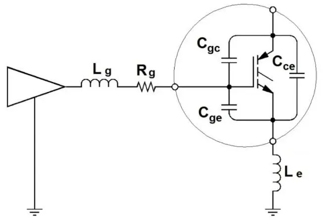
GaN has a wider bandgap (about 3.4 eV versus 1.1 eV for silicon), allowing operation at higher voltages before dielectric breakdown. That enables both higher-power and higher-voltage operation with improved efficiency. High electron mobility further permits GaN operation at much higher frequencies, making it well suited for RF power applications that push beyond the GHz range where silicon struggles.
Thermal and scaling considerations
Because silicon has slightly better thermal conductivity, GaN devices can impose larger heat-sinking requirements than equivalent silicon parts. This limits how small GaN devices can be made for a given high-power application, since additional material or cooling is needed to manage heat.
The P-type GaN problem
Despite its advantages, GaN has a fundamental limitation: current commercial GaN devices are predominantly N-type. That forces designers into NMOS-only topologies, which has important implications for many applications.
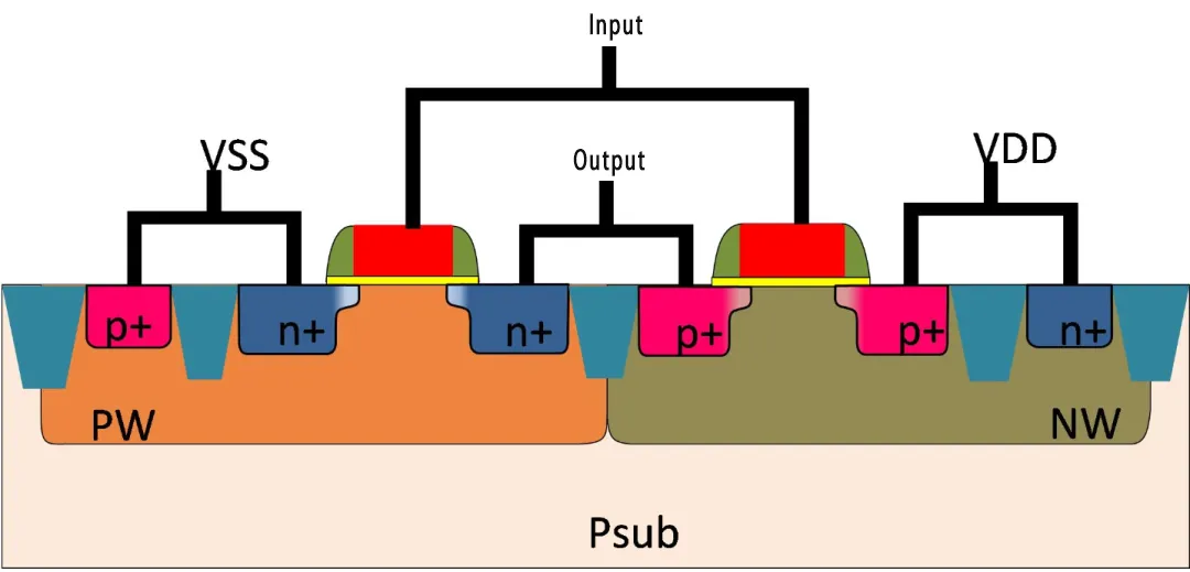
To illustrate, NMOS logic was popular in the 1970s and 1980s because of its manufacturing simplicity. NMOS gates use a resistor between the supply and the drain of an N-type MOS transistor, so the transistor gate can control the drain voltage and implement logic. However, NMOS relies on resistive pull-ups, so when the transistor is on substantial power is wasted in the resistor. At scale, this static power loss becomes significant.
Complementary MOS (CMOS) logic uses both P-type and N-type transistors operating in opposition, so outputs are never directly connected between supply and ground except during switching. That arrangement dramatically reduces static power dissipation; the only substantial power loss occurs briefly during transitions when complementary devices provide a momentary path between supply and ground.
Because commercial GaN today is essentially N-type, GaN-based digital logic would be limited to NMOS-style designs with their higher static power dissipation. For RF amplifiers this is less of an issue, but for logic and many power-management applications the absence of P-type GaN is a major drawback.
Why making P-type GaN is hard
P-type GaN devices are possible in principle and have been used in optical devices such as blue LEDs. However, the implementations suitable for optoelectronics are not ideal for digital logic or power electronics. Magnesium is the only practical p-type dopant for GaN, but high concentrations are required and hydrogen easily incorporates into the structure during annealing, degrading performance. These material and process challenges have so far prevented widely available, high-performance P-type GaN devices for logic and power applications.
Implications for device design
The lack of P-type GaN limits the ability to fully exploit GaN’s potential. Designers must use alternative approaches, such as combining GaN with P-type silicon MOS transistors to achieve complementary behavior. While that provides some complementary capability, it constrains the frequency and efficiency advantages that GaN can offer because the overall system remains limited by the silicon devices.
Alternatives and outlook
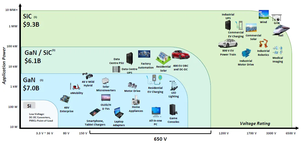
Other wide-bandgap materials are under active research. Silicon carbide (SiC) is another major contender for power applications: like GaN, SiC supports higher voltages, higher breakdown fields, and better conductivity than silicon, and its superior thermal conductivity makes it suitable for extreme-temperature operation while handling large power in compact sizes. Unlike GaN, SiC is less suitable for very-high-frequency RF applications, so GaN remains the preferred option for compact RF power amplifiers.
Future progress may produce practical P-type GaN devices or complementary technologies that pair effectively with GaN. Until then, GaN will continue to offer important advantages while being constrained by the absence of widely available P-type devices.
Research needs
Overcoming GaN’s current limitations will require interdisciplinary work across materials science, electrical engineering, and physics. Breakthroughs that enable reliable P-type GaN or identify complementary materials that integrate well with GaN could significantly enhance GaN-based device performance and broaden its role in energy-efficient, compact, and reliable electronic systems.