 ALLPCB


Introduction
In high-frequency PCB designs, vias serve as critical interconnects between layers, enabling complex routing in multilayer boards. However, these structures introduce challenges that can compromise signal integrity, particularly as frequencies exceed 1 GHz. Engineers must optimize via placement, via size, and manage via stubs to minimize impedance discontinuities and maintain clean signal transmission. Poor via optimization leads to reflections, crosstalk, and insertion loss, degrading overall performance in applications like 5G, radar, and high-speed data interfaces. This article explores structured strategies for via optimization, drawing on established engineering principles to guide electric engineers in achieving robust designs. By focusing on practical techniques such as backdrilling, designers can enhance signal integrity without excessive complexity.
Understanding Vias and Their Role in High-Frequency PCBs
Vias are plated through-holes that provide vertical electrical connections in PCBs, categorized as through-hole, blind, or buried based on their depth. In high-frequency environments, every via represents a potential impedance discontinuity due to its parasitic inductance and capacitance. These parasitics arise from the via barrel's geometry and the abrupt transition from trace to via, disrupting the controlled impedance of transmission lines. Signal integrity suffers when these discontinuities cause return loss or eye diagram closure, especially for signals with fast rise times. Optimizing vias requires balancing electrical performance with manufacturability constraints, such as drill aspect ratios and plating uniformity. Industry standards like IPC-2221 outline baseline requirements for via dimensions and annular rings to ensure reliability.
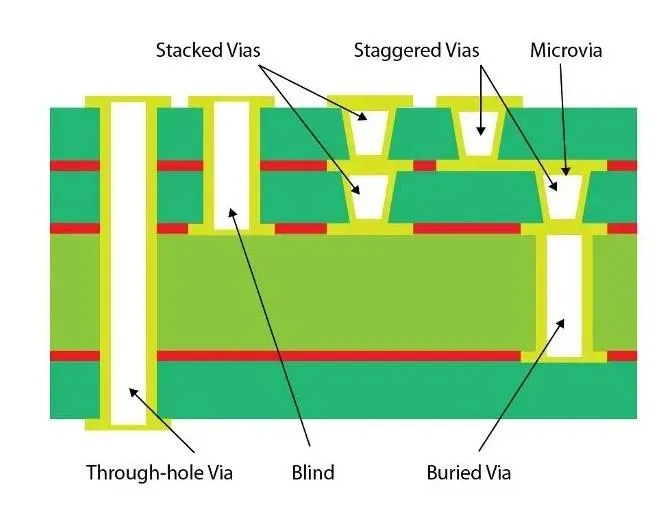
Via stubs, the unused portions of through-hole vias extending beyond the signal path, exacerbate these issues by acting as resonant antennas. At high frequencies, stubs generate standing waves that reflect energy back toward the source, leading to bit errors in digital signals. The length of the stub determines its resonant frequency, making stub management essential in dense multilayer boards. Engineers evaluate stub effects through time-domain reflectometry or frequency-domain simulations to quantify impacts on insertion loss and return loss. Proper via selection, such as preferring blind vias where possible, reduces stub lengths inherently. This foundational understanding sets the stage for targeted optimization strategies.
The Impact of Via Placement on Signal Integrity
Strategic via placement minimizes crosstalk and maintains reference plane integrity, crucial for high-frequency signal integrity. Placing vias too close to each other increases capacitive coupling, while poor alignment with traces introduces additional inductance. For differential pairs, symmetric via placement ensures balanced paths, preventing skew and common-mode noise conversion. Optimal via placement positions them as close as possible to component pads to shorten transition lengths, reducing loop inductance. Ground return paths should remain continuous under vias to avoid splits that cause impedance bumps.
In multilayer boards, via placement must consider layer transitions to preserve signal return paths adjacent to the signal trace. Avoiding via placement over plane splits prevents ground bounce and EMI radiation. Simulations reveal that via-to-via spacing greater than three times the trace width helps isolate signals effectively. These practices align with general design guidelines to control electromagnetic fields around vias.
Optimizing Via Size for Impedance Control
Via size directly influences parasitic effects, with smaller diameters reducing inductance but challenging fabrication tolerances. Larger vias offer lower resistance for power delivery but introduce higher inductance in signal paths, creating impedance discontinuities. Engineers select via size based on the required characteristic impedance, often targeting drill diameters that match trace widths proportionally. Annular ring dimensions, as specified in standards like IPC-6012E, ensure plating integrity and prevent breakout during thermal stress.
The inductance of a via scales with its length and inversely with diameter, following approximate formulas derived from transmission line theory. Capacitance arises from the anti-pad clearance in reference planes, necessitating precise anti-pad sizing to tune the via's input impedance. For high-frequency designs, microvias with diameters under 0.15 mm minimize parasitics while supporting HDI densities. Balancing via size with board thickness maintains aspect ratios suitable for uniform plating.
Trade-offs include drill accuracy and cost, as finer vias demand laser drilling or advanced processes. Field solvers help predict via impedance profiles, guiding iterative sizing.
Mitigating Via Stubs Through Advanced Techniques
Via stubs in through-hole designs extend beyond active layers, causing severe signal integrity degradation at frequencies where stub length approaches a fraction of the wavelength. Reflections from stub ends create nulls in the frequency response, attenuating harmonics essential for fast edges. Quantifying stub impact involves calculating the stub's quarter-wave resonance, beyond which it acts as a short or open circuit alternately.
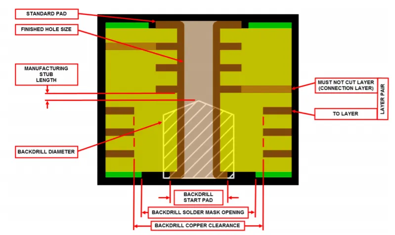
Backdrilling emerges as a primary solution, mechanically removing the unused stub after plating. This controlled depth drilling targets specific layers, leaving a clean signal path with minimal residue. Backdrilling tolerances typically require 0.1 mm setbacks from landing pads to avoid damage, ensuring plating barrel integrity. The process adds steps but significantly improves return loss by 10-20 dB in critical nets.
Blind and buried vias eliminate stubs by design, connecting only required layers, though they increase layer count and cost. Via-in-pad configurations further optimize density but demand precise fill and planarization.
Additional Best Practices for Via Optimization
Beyond basics, via fencing with ground vias shields high-speed signals, reducing far-end crosstalk by providing low-impedance return paths. Stitch vias along trace edges tie planes together, minimizing slot radiation. Anti-pad enlargement tunes via capacitance to compensate for inductance, achieving broadband impedance matching.
Layer stackup planning influences via performance, with symmetric builds reducing warpage and maintaining plane proximity. Pre-emphasis and equalization in drivers complement via optimization but cannot fully compensate discontinuities. Fabrication notes specify backdrill depths and tolerances clearly.
Practical Implementation and Troubleshooting
In practice, engineers prototype via structures in test coupons to validate signal integrity before full layout. Eye diagrams and TDR measurements identify problematic vias, correlating to simulations. Common issues include backdrill breakout, addressed by conservative depth specs, or plating voids from high aspect ratios.
Case studies show backdrilling enabling 25 Gbps+ SerDes links by removing 0.5 mm stubs, restoring eye height. Troubleshooting via stubs involves shortening paths or converting to blind vias where routing allows.
Conclusion
Optimizing vias in high-frequency PCB designs demands a holistic approach to via placement, via size, stub management, and backdrilling to preserve signal integrity. By minimizing impedance discontinuities through structured techniques, engineers achieve reliable performance in demanding applications. Adhering to standards like IPC-2221 and IPC-6012E ensures manufacturability alongside electrical goals. Integrating these strategies early in the design flow yields cost-effective, high-yield boards. Continuous simulation and validation refine outcomes, empowering electric engineers to push frequency limits confidently.
FAQs
Q1: What is the main impact of via stubs on signal integrity in high-frequency PCBs?
A1: Via stubs cause reflections and resonances that distort signals, leading to eye closure and bit errors. These unused via portions act as antennas, particularly problematic above 1 GHz. Mitigation via backdrilling or blind vias restores clean transmission paths. Proper stub length control per design guidelines prevents impedance discontinuities.
Q2: How does via placement affect impedance discontinuity?
A2: Via placement influences coupling and return path continuity, directly impacting impedance profiles. Close spacing increases crosstalk, while misalignment adds inductance. Optimal placement near pads and symmetric for pairs minimizes discontinuities. Ground plane adjacency further stabilizes impedance for high-speed signals.
Q3: Why is backdrilling essential for via optimization in multilayer high-frequency designs?
A3: Backdrilling removes via stubs, eliminating reflections that degrade signal integrity. It enables through-hole vias in dense stacks without blind via costs. Precise depth control ensures clean transitions, improving return loss significantly. This technique suits frequencies where stub lengths exceed tolerable limits.
Q4: What considerations guide via size selection for signal integrity?
A4: Via size balances inductance reduction with fabrication feasibility, tuning parasitics to match line impedance. Smaller sizes lower inductance but require advanced drilling. Annular rings and anti-pads adjust capacitance accordingly. Simulations validate choices against measured performance.
References
IPC-2221 — Generic Standard on Printed Board Design. IPC
IPC-6012E — Qualification and Performance Specification for Rigid Printed Boards. IPC, 2017
IPC-A-600K — Acceptability of Printed Boards. IPC, 2020


