 ALLPCB


Introduction
Non-uniform solder mask application remains one of the most persistent challenges in printed circuit board fabrication. When the protective coating varies in thickness across a panel, it can compromise insulation integrity, adhesion strength, and long-term reliability. Engineers and manufacturing teams must address these variations early because they directly affect assembly yields and field performance. Logical process mapping helps identify where deviations occur in the coating sequence. Structured analysis of material behavior and equipment parameters provides the foundation for consistent results.
What Is Uneven Solder Mask Thickness and Why It Matters
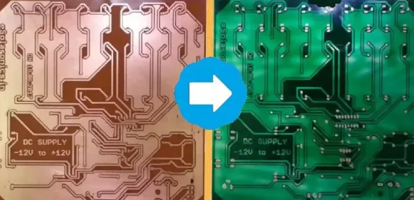
Uneven solder mask thickness describes localized differences in the cured coating depth on a PCB surface. These variations may appear as thin spots over traces or thicker accumulations in recessed areas. Industry standards require minimum insulation distances that become unreliable when coating uniformity falls outside acceptable limits. Procurement teams and design engineers recognize that such inconsistencies increase the risk of electrical shorts or delamination during thermal cycling. Factory-driven monitoring of coating parameters therefore supports both quality targets and cost control. Consistent thickness also simplifies downstream processes such as stencil printing and component placement.
Technical Principles and Mechanisms Behind Non-Uniform Coating
Solder mask application relies on precise control of liquid or dry-film deposition followed by controlled curing. Viscosity changes during flow can cause the material to pool in low-lying regions while leaving raised conductors with reduced coverage. Substrate topography, including copper trace height and via fill levels, influences how the coating spreads before exposure. Temperature gradients across the panel during pre-bake or final cure further contribute to differential shrinkage. Engineers apply structured troubleshooting by mapping each process variable to observed thickness profiles. This methodical approach isolates whether the root cause lies in surface preparation, application equipment settings, or environmental conditions.
Related Reading: PCB Direct Imaging and Solder Mask Application: A Comprehensive Guide
Practical Solutions and Best Practices for Improved Uniformity
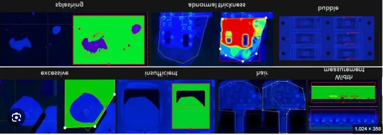
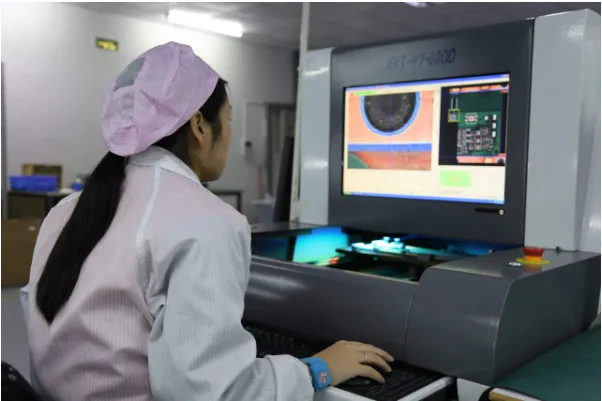
Process control begins with standardized surface preparation that removes contaminants and ensures consistent wettability. Application techniques such as curtain coating or electrostatic spraying allow finer adjustment of deposit volume compared with older screen-printing methods. Engineers monitor key parameters including belt speed, spray pressure, and gap distance using statistical process control charts. Post-application inspection with automated optical systems or micrometer measurements provides immediate feedback for corrective action. Adherence to IPC-A-600K guidelines establishes visual and dimensional acceptance criteria that guide these adjustments. Regular calibration of curing ovens maintains uniform thermal profiles across the entire panel.
Troubleshooting Insights for Electric Engineers
When thickness variations are detected, engineers first review panel layout symmetry and copper distribution to rule out design-related contributors. Next, they examine application equipment for nozzle wear or pressure fluctuations that disrupt even flow. Comparative testing of alternative coating sequences often reveals whether switching from liquid to dry-film methods reduces variability in high-density areas. Documentation of each trial run supports root-cause analysis and prevents recurrence in subsequent builds. This logical sequence keeps troubleshooting efficient while preserving production throughput.
Related Reading: Top 5 Solder Mask Mistakes to Avoid in Your PCB Assembly Projects
Conclusion
Uniform solder mask application protects circuit integrity and supports reliable assembly outcomes. Systematic attention to material behavior, equipment settings, and inspection protocols reduces the incidence of thickness variations. Electric engineers benefit from structured evaluation frameworks that link observed defects to controllable process factors. Consistent implementation of these practices aligns manufacturing results with established industry expectations.
FAQs
Q1: What causes uneven solder mask thickness during the PCB manufacturing process control stage?
A1: Variations in coating thickness often stem from differences in substrate topography, inconsistent material viscosity, or fluctuations in application equipment parameters. Engineers trace these issues through sequential process audits that compare panel-to-panel results. Maintaining stable environmental conditions and regular equipment calibration helps limit the occurrence of such defects.
Q2: How do solder mask coating problems affect long-term PCB reliability?
A2: Non-uniform coverage can reduce dielectric strength between conductors and increase the likelihood of moisture ingress or delamination. These conditions become evident during thermal or humidity testing when insulation resistance drops below required thresholds. Early detection through thickness mapping prevents downstream assembly failures.
Q3: Which solder mask application techniques improve coating uniformity?
A3: Techniques such as controlled curtain coating or optimized spray parameters allow more even distribution across varying copper heights. Engineers evaluate each method against target thickness tolerances before full-scale production. Process validation confirms that the chosen technique meets acceptance criteria across multiple panel lots.
Q4: What steps support improving solder mask uniformity in high-volume production?
A4: Implementation of statistical process control combined with automated thickness measurement provides continuous feedback for parameter adjustments. Training operators on standardized setup procedures further reduces human-induced variation. Periodic audits against IPC-SM-840 requirements verify that uniformity targets remain achievable.
References
IPC-A-600K — Acceptability of Printed Boards. IPC, 2020
IPC-SM-840E — Qualification and Performance Specification of Permanent Solder Mask and Flexible Cover Materials. IPC, 2010
IPC-6012E — Qualification and Performance Specification for Rigid Printed Boards. IPC, 2017


