 ALLPCB


If you're involved in PCB assembly projects, avoiding solder mask errors is critical to ensuring the reliability and functionality of your boards. Solder mask mistakes can lead to costly PCB assembly failures, delays, and performance issues. In this comprehensive guide, we’ll explore the top 5 common solder mask mistakes, provide actionable tips for avoiding solder mask problems, and share insights on solder mask troubleshooting to help you achieve flawless results.
Whether you're a seasoned engineer or new to PCB design, understanding these pitfalls and how to prevent them will save you time, money, and frustration. Let’s dive into the details of these errors and how to address them effectively.
What Is a Solder Mask and Why Does It Matter?
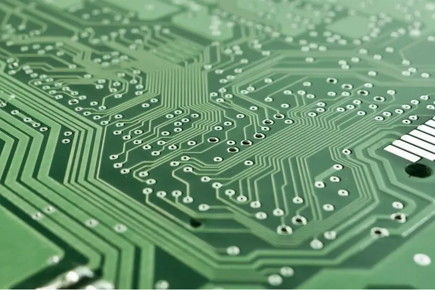
Before we get into the common solder mask mistakes, let’s clarify what a solder mask is and why it’s so important in PCB assembly. A solder mask is a thin protective layer of polymer applied to the surface of a printed circuit board (PCB). Its primary role is to shield the copper traces from oxidation, prevent solder bridges during assembly, and provide electrical insulation between components.
Without a properly applied solder mask, your PCB is at risk of short circuits, corrosion, and other failures that can compromise the entire project. However, even a small error in the solder mask application or design can lead to significant issues. That’s why identifying and avoiding solder mask problems is essential for successful PCB assembly.
Top 5 Solder Mask Mistakes to Avoid in PCB Assembly
Now, let’s explore the top 5 solder mask errors that can derail your PCB assembly projects. We’ll break down each mistake, explain why it happens, and offer practical solutions for avoiding these issues.
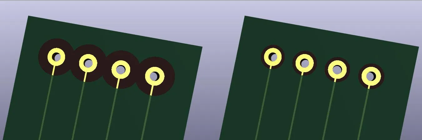
1. Inappropriate Solder Mask Clearances
One of the most common solder mask mistakes is setting incorrect clearances around pads and vias. Solder mask clearance refers to the area around a pad or via where the mask is removed to allow soldering. If the clearance is too small, the solder mask may overlap the pad, making it difficult to solder components properly. If it’s too large, it can expose unnecessary copper, increasing the risk of short circuits or corrosion.
For example, a typical clearance for surface-mount pads should be around 0.05 mm to 0.1 mm larger than the pad size to ensure proper soldering without overlap. Failing to adhere to these tolerances can lead to assembly failures, especially in high-density designs where precision is critical.
How to Avoid This Problem:
- Always double-check your design rules in your PCB layout software to ensure clearances meet manufacturing specifications.
- Consult with your PCB manufacturer to confirm their minimum clearance requirements, as these can vary based on equipment and processes.
- Use automated design rule checks (DRC) to catch clearance errors before sending your design for production.
2. Incomplete Via Tenting
Via tenting refers to covering vias (small holes that connect different layers of a PCB) with solder mask to protect them from solder flow or environmental damage. Incomplete or missing via tenting is a frequent solder mask error that can cause solder to wick into the via during assembly, leading to weak joints or short circuits. It can also expose the via to moisture and contaminants, reducing the board’s lifespan.
Incomplete tenting often occurs due to design oversights or manufacturing limitations, especially with smaller vias (e.g., diameters below 0.3 mm), where the solder mask may not fully cover the opening.
How to Avoid This Problem:
- Specify in your design whether vias should be tented, plugged, or left open based on their function and location.
- Work with your manufacturer to ensure they can achieve full tenting for your via sizes, as some processes may require additional steps like via plugging.
- Inspect Gerber files before production to confirm that via tenting is correctly defined in the solder mask layer.
3. Solder Mask Misalignment
Solder mask misalignment happens when the mask layer is not properly aligned with the copper traces and pads on the PCB. This can result in exposed copper areas that should be protected or covered pads that should be exposed for soldering. Misalignment is often caused by errors in the design file, inaccuracies during manufacturing, or improper registration of layers.
For instance, a misalignment of just 0.1 mm can expose critical traces near high-voltage areas, increasing the risk of arcing or short circuits. This issue can be particularly problematic in high-frequency designs where signal integrity is crucial.
How to Avoid This Problem:
- Ensure your design files are accurate and include proper alignment markers (fiducials) to guide the manufacturing process.
- Verify that your manufacturer has robust quality control processes to detect and correct misalignment during production.
- Request a prototype run for complex designs to identify potential alignment issues before full-scale production.
4. Overlapping Silkscreen and Solder Mask
The silkscreen layer on a PCB is used to print labels, symbols, and component identifiers for assembly and testing. However, a common mistake is allowing the silkscreen to overlap with the solder mask openings, such as pads or vias. This can obscure critical areas, making soldering difficult or leading to errors during assembly.
This issue often arises when designers fail to account for manufacturing tolerances or when silkscreen text is placed too close to pads. For example, if silkscreen ink covers a pad with a 0.5 mm diameter, it can prevent proper solder adhesion, leading to weak connections.
How to Avoid This Problem:
- Maintain a minimum distance (typically 0.2 mm) between silkscreen elements and solder mask openings in your design.
- Use design software features to automatically check for silkscreen overlap during the layout phase.
- Review the final Gerber files to ensure no silkscreen elements interfere with solderable areas.
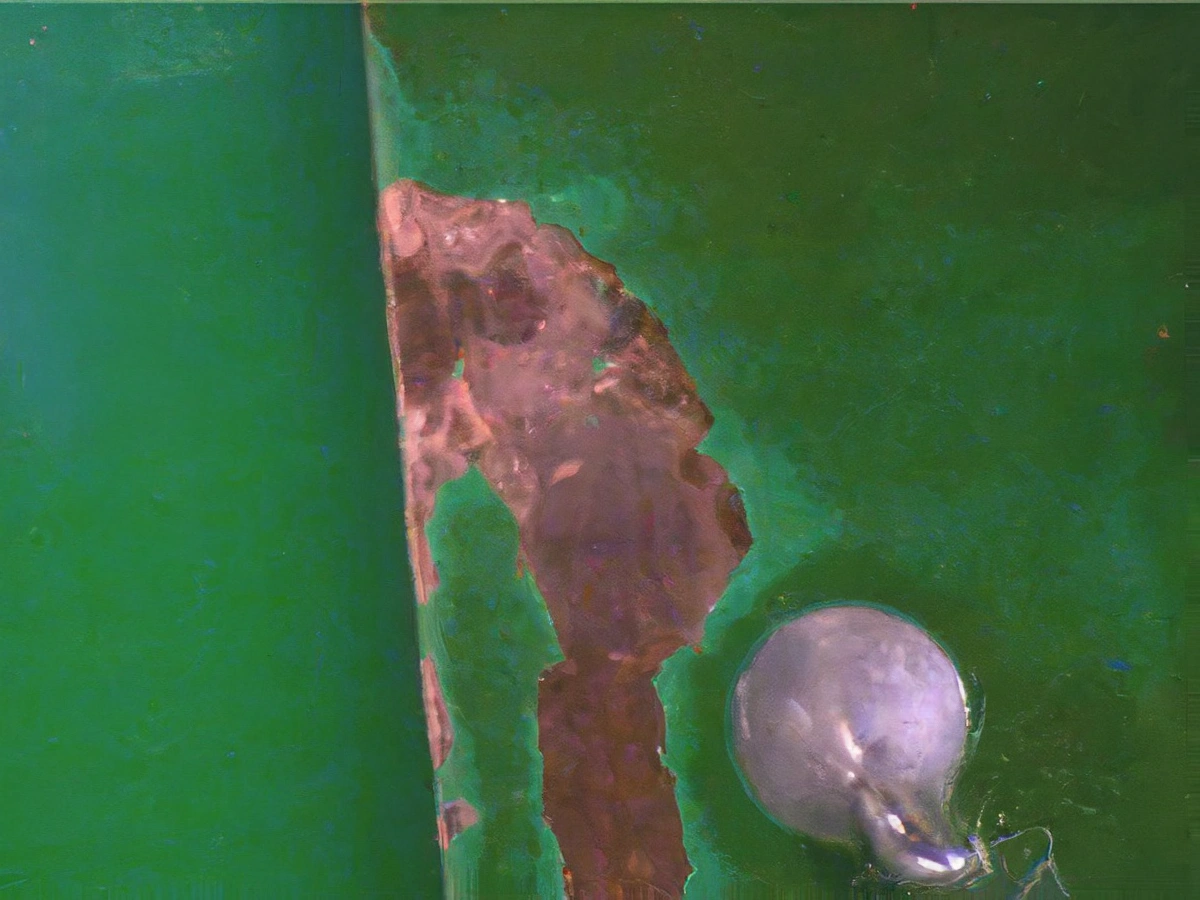
5. Poor Solder Mask Adhesion or Curing Issues
Solder mask adhesion and curing problems can lead to peeling, cracking, or delamination of the mask layer over time. This exposes copper traces to environmental factors like moisture and oxidation, increasing the risk of PCB assembly failures. Poor adhesion is often caused by contamination on the PCB surface, improper curing temperatures, or low-quality solder mask materials.
For example, if the solder mask is not cured at the recommended temperature range (typically 120°C to 150°C for 20-30 minutes), it may not bond properly to the board, leading to flaking during assembly or use.
How to Avoid This Problem:
- Ensure the PCB surface is clean and free of contaminants like oil or dust before applying the solder mask.
- Confirm that your manufacturer follows the correct curing process, including temperature and duration, for the specific solder mask material used.
- Conduct adhesion tests, such as the tape test, on prototype boards to verify the solder mask’s durability before full production.
Solder Mask Troubleshooting: How to Identify and Fix Issues
Even with careful planning, solder mask errors can still occur during PCB assembly. Knowing how to troubleshoot these issues is key to minimizing delays and costs. Below are some practical solder mask troubleshooting tips to help you identify and resolve problems quickly.
- Visual Inspection: Use a magnifying glass or microscope to check for misalignment, incomplete tenting, or adhesion issues. Look for exposed copper or uneven mask application.
- Adhesion Testing: Perform a simple tape test by applying adhesive tape over the solder mask and peeling it off. If the mask lifts, there’s an adhesion problem that needs addressing.
- Electrical Testing: Use a multimeter to check for short circuits or open connections that may indicate solder mask failures like exposed traces or solder bridges.
- Collaboration with Manufacturer: If issues persist, work closely with your PCB manufacturer to review the production process and identify whether the error originated in design or fabrication.
Why Avoiding Solder Mask Problems Saves Time and Money
Solder mask errors can lead to significant setbacks in PCB assembly projects. A single mistake, such as poor adhesion or misalignment, can result in defective boards that fail during testing or in the field. This not only increases production costs due to rework or scrap but also delays project timelines, potentially harming your reputation with clients or stakeholders.
By focusing on avoiding solder mask problems from the design stage through to manufacturing, you can achieve higher yields and more reliable boards. For instance, investing time in design rule checks (DRC) can prevent issues like incorrect clearances, saving you from costly revisions later. Similarly, clear communication with your manufacturer about via tenting or curing requirements can reduce the likelihood of assembly failures.
Best Practices for Flawless Solder Mask Application
To wrap up, here are some overarching best practices to ensure your solder mask application is error-free and your PCB assembly projects run smoothly:
- Thorough Design Review: Always validate your design files using automated tools and manual checks to catch potential solder mask errors early.
- Manufacturer Collaboration: Share detailed specifications and requirements with your PCB manufacturer to align on processes like curing and alignment.
- Prototype Testing: Build and test prototypes to identify solder mask issues before committing to large-scale production.
- Stay Updated on Standards: Keep up with industry standards like IPC-SM-840 for solder mask performance to ensure your designs meet quality benchmarks.
Conclusion
Solder mask mistakes can have a big impact on the success of your PCB assembly projects, but they are avoidable with the right knowledge and practices. By understanding the top 5 common solder mask mistakes—inappropriate clearances, incomplete via tenting, misalignment, silkscreen overlap, and poor adhesion—you can take proactive steps to prevent PCB assembly failures. Use the solder mask troubleshooting tips and best practices shared in this guide to enhance the reliability and performance of your boards.
With careful attention to design details and strong collaboration with your manufacturing partner, you can sidestep these pitfalls and deliver high-quality PCBs that meet your project goals. Start implementing these strategies today to ensure your next PCB assembly project is a success.


