 ALLPCB


When reviewing a MOSFET datasheet, you need to know what to look for. Some parameters are prominent and straightforward (BVDSS, RDS(ON), gate charge), while others are vague or ambiguous (IDA, SOA curves), and a few are of limited practical use (for example: switching times). In this multipart article series, the goal is to demystify MOSFET datasheets so engineers can find and interpret the parameters that matter for their applications, and avoid being misled by specmanship from different manufacturers.
1 UIS / Avalanche Rating
The un-clamped inductive switching (UIS) rating has been a widely used datasheet item since the mid-1980s and remains a useful metric. Although repeated avalanche operation is not recommended in real applications, designers use UIS ratings during device selection and qualification to avoid vulnerable parts. Devices with especially weak UIS performance across temperature or with severe degradation over temperature (for example, more than 30% degradation between 25°C and 125°C) should be avoided because they are more prone to failure. Designers should also be wary of manufacturers overstating avalanche capability in their ratings.
The UIS test is performed with the test circuit shown below. A supply voltage is applied across the MOSFET while it is off and leakage is checked. While the MOSFET is on, current through the inductor increases. When the desired current is reached, the MOSFET is turned off and the L di/dt voltage spike exceeds the MOSFET breakdown voltage, activating the intrinsic parasitic bipolar transistor and producing an effective avalanche event on the device. The test is repeated with progressively higher current until the initial leakage test fails, indicating device damage.
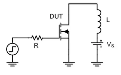
The avalanche energy is calculated with the equation E = 1/2 L I^2. This is the starting point for the test. By changing the inductor size you change the stress applied to the device under test. Predictably, a larger inductor reduces the UIS current required to damage the MOSFET. That lower current is not fully offset by the larger inductance in the energy equation, so the computed energy actually increases even though the current decreases. The table below illustrates this relationship using data collected from a TI CSD18502KCS 60 V NexFET power MOSFET.
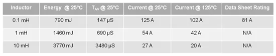
Using the smallest inductor in the test (0.1 mH) produces the highest stress and highest currents. TI uses a 0.1 mH inductor to test production devices and reports the associated energy value in the datasheet. Because there is no firm industry standard for this value, some manufacturers use larger inductors in their UIS tests to make their devices appear to have higher avalanche energy. Designers should therefore be cautious when comparing avalanche ratings and always ask for the specific UIS test conditions when comparing devices from different suppliers.
2 Safe Operating Area (SOA) Plot
Aside from current ratings, the safe operating area (SOA) curve is one of the most frequently asked-about items on a power MOSFET datasheet. Understanding SOA requires care because each supplier may generate SOA curves differently, and the usefulness of the curve depends on the reader's understanding of the underlying test conditions and limits.
Although MOSFETs see maximum value in some hot-swap or linear-region applications, SOA curves are increasingly used by motor-drive and supply designers as an indicator of overall robustness and the device's ability to handle high power.
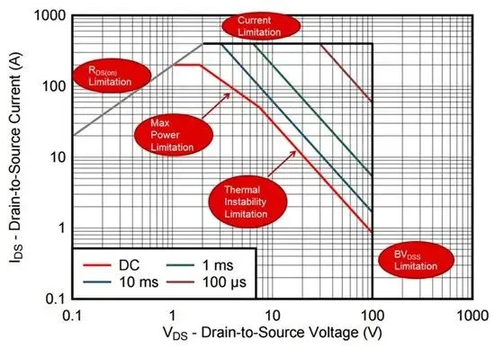
An SOA curve can be drawn from five distinct limiting conditions, each shaping sections of the curve. Four of those curves—RDS(on) limit, current limit, peak power limit, and BVDSS limit—can be plotted from known device parameters. The remaining region, thermal instability, is more problematic. This portion of the SOA deviates from a constant-power line (which has slope –1 on log-log axes) and the deviation indicates thermal runaway; the steeper the slope, the more likely the device will enter thermal instability at higher breakdown voltages. When suppliers attempt to estimate this region, they may overstate device current capability or be conservative, because the slope of the thermal-instability line cannot be known without measurement.
TI has one of the most capable SOA testers, able to push kilowatts through a device in pulse durations as short as 100 μs. To produce the datasheet curve, devices are driven to failure at a series of voltages and pulse durations; each plotted point represents a forced failure of a CSD19536KTT device. From these measured failure points, the slope and position of the thermal-instability line can be determined.
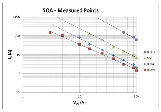
As a reliability margin, measured thermal-instability lines are derated by 30%–40% at arbitrary positions to account for part-to-part variation. When comparing SOA plots across vendors, be aware that not every supplier applies such derating or reports the underlying failure points. Without base data showing where parts actually failed, it is difficult to judge which part is more reliable solely from the datasheet SOA curve.
In part 3 of this series I will explain the current ratings that appear on the first page of MOSFET datasheets, show how those ratings are derived, and discuss their practical implications for designers.
3 Continuous Current Ratings
Now we will discuss MOSFET current ratings and how they can be misleading. These ratings are often not measured in the same way as parameters like RDS(ON) or gate charge; instead they are sometimes calculated, and there are multiple methods to derive them.
Most parts include a package current rating, which is largely independent of ambient conditions and is a function of the internal connections between the silicon chip and the plastic package. Exceeding this rating will not immediately damage the MOSFET, but sustained operation above it will reduce lifetime. Failure mechanisms above this limit include bond-wire fusing, thermal degradation of molding compounds, and electromigration stress.
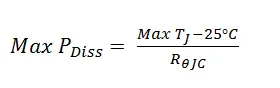
There is also a chip limit, typically specified with the case temperature held at 25°C. This condition assumes an ideal heatsink and uses only junction-to-case thermal resistance to compute the maximum power the device can handle. In other words, it assumes Rθcase-to-ambient is zero, which is not realistic in many applications. Treat the chip limit as a figure of merit that reflects RDS(ON) and thermal resistance rather than a practical continuous current rating for most systems.
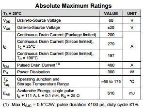
Figures 1a and 1b show the absolute maximum ratings tables from the front pages of the CSD18536KCS and CSD18535KCS 60 V TO-220 MOSFET datasheets. Both parts list a package rating of 200 A, but the CSD18536KCS has a lower RDS(ON) and lower thermal resistance, resulting in a higher chip limit of 349 A. That indicates it should run cooler than the CSD18535KCS for the same continuous current. Still, it is not recommended to run either device for extended periods above 200 A. From the MOSFET perspective, that implies any current pulse longer than about 100 ms; pulses longer than this are essentially DC pulses.
Some QFN datasheets include a third continuous current rating calculated like the chip limit but using the measured RθJA. Using RθJA (for a standard SON5x6 package a typical value is 40°C/W) to compute maximum power assumes the QFN only dissipates a few watts in the application, so this method gives a more practical DC current limit for QFN parts that are not exposed to heat-sinking.
In part 4 of this series I will provide a similar analysis for pulse current ratings, IDM, and relate that rating to other datasheet parameters including SOA.
4 Pulse Current Ratings
This section covers pulse current ratings, how they are calculated, and how they appear on the SOA plot.
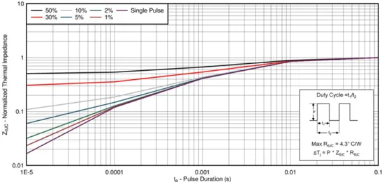
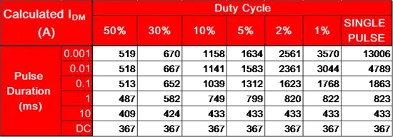
The datasheet pulse current rating (IDM) is similar to the continuous current rating in that it is a theoretical value. Unlike the continuous rating, IDM is calculated as a thermal constraint function using transient thermal impedance for the specified pulse duration and the duty cycle noted in the absolute maximum ratings table footnote. For example, the CSD17579Q5A 30 V N-channel MOSFET datasheet specifies a maximum pulse current of 105 A for pulse durations ≤ 100 μs and duty cycle ≤ 1%. To determine the transient thermal impedance used for IDM calculation, refer to the normalized transient thermal impedance curve.
Using the transient thermal impedance and computing the maximum current as for the continuous case yields a thermal-limited current of 119 A. But the datasheet specifies 105 A. Looking at the SOA for that device, the 100 μs line intersects the RDS(ON) limit before reaching 119 A; that intersection occurs at 105 A. In this case the RDS(ON) physical limit constrains the device before the thermal limit is reached, so the absolute maximum pulse current is reduced accordingly.
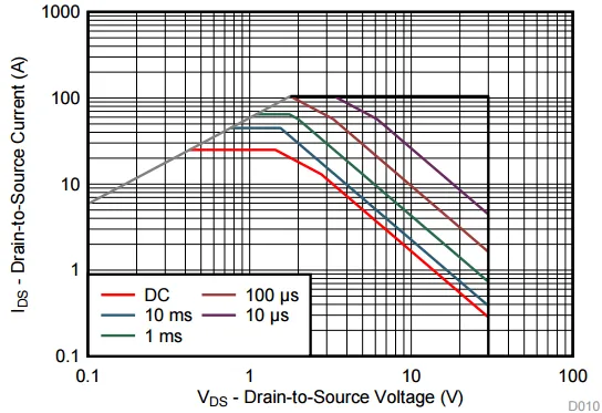
For each major pulse duration shown on the SOA, a current limit is computed (provided the RDS(ON) limit is not reached first); these computed limits define the upper envelope of the curves.
Because absolute maximum currents are theoretical, manufacturers typically seek hard data before release to validate the device capability. Practical lab limits often cap the maximum pulse current that can be demonstrated; in this case test setups limit pulse currents to about 400 A, which becomes an artificial upper bound used internally. Some suppliers publish similar caps, while others do not. For example, TI does not publish IDM values above 400 A. The calculated IDM for parts with extremely low RDS(ON) and thermal resistance, such as the CSD17570Q5B, can be much larger than practical testable currents, which illustrates how theoretical calculations can produce unrealistically large ratings if practical limits and pulse conditions are not carefully considered.
In part 5 I will present further analysis of pulse current ratings (IDM) and show how they relate to other datasheet parameters, including SOA.
5 Switching Parameters
Finally, this installment considers several mixed switching parameters that appear on MOSFET datasheets and evaluates their relevance to overall device performance. Output charge of the intrinsic diode (QOSS) and reverse recovery charge (Qrr) are key contributors to switching losses in many high-frequency power applications. However, designers must be careful when comparing these parameters between suppliers because test conditions determine the results.
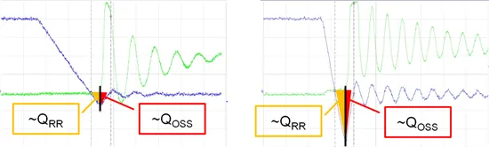
Qrr can be strongly dependent on the diode forward current (If) used in the test. Some vendors do not list QOSS separately and instead include it within Qrr specifications. Beyond the listed test conditions, other factors such as PCB parasitic inductance and subjective measurement techniques make direct comparison across vendors difficult. This does not mean these parameters are unimportant; rather, it means that reliable comparison requires independent measurements using consistent methods and circuit boards.
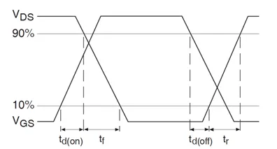
The last set of parameters I will mention are switching times. These four parameters are typically defined by the waveform shown below and appear on every vendor's datasheet. They are highly dependent on PCB layout and test conditions, which is why experienced engineers often regard them as among the least useful datasheet numbers. Intended to indicate switching speed, they are actually limited by driver strength and leakage, and therefore at best reflect those conditions. Gate charge parameters and the internal gate resistance, Rg, are far better indicators of a device's real switching behavior since they are less affected by specmanship in test conditions.
This series has covered common MOSFET datasheet parameters and how to interpret them in design. Use measured data and consistent test methods when comparing devices from different suppliers, and be cautious of theoretical limits that do not reflect application conditions.


