ALLPCB


Introduction
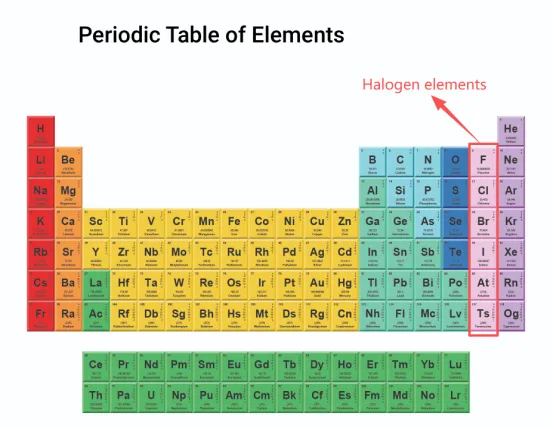
Halogen-free PCB manufacturing has gained significant traction in recent years as electronics industries prioritize environmental compliance and worker safety. These boards eliminate halogens like chlorine and bromine from base materials, primarily laminates and resins, to reduce toxic emissions during combustion. Despite their growing adoption, several halogen-free PCB myths persist among engineers and procurement teams, often stemming from early material limitations or incomplete understanding of modern formulations. Debunking halogen-free PCB misconceptions is essential for informed decision-making in design and production. This article addresses the top five misconceptions, drawing on factory insights and industry practices to clarify facts.
What Are Halogen-Free PCBs and Why Do They Matter?
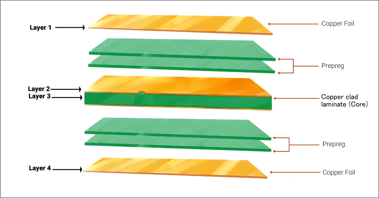
A halogen-free PCB contains less than 900 ppm of chlorine or bromine individually, and total halogens below 1500 ppm, as defined by common industry specifications. This threshold ensures minimal environmental impact while maintaining functionality comparable to traditional FR-4 materials. Factory processes replace brominated flame retardants with phosphorus or nitrogen-based alternatives in resins and prepregs. The shift matters because regulations increasingly demand reduced hazardous substances, and end-users in consumer electronics, automotive, and telecommunications seek safer products. In manufacturing, halogen-free boards support sustainability goals without sacrificing assembly yields when processes are optimized. Engineers benefit from understanding these materials to avoid unnecessary trade-offs in reliability or cost.
Top 5 Misconceptions About Halogen-Free PCB Manufacturing
Misconception 1: Halogen-Free PCBs Are Prohibitively Expensive
Many engineers assume the cost of halogen-free PCBs remains significantly higher due to specialized materials, leading to hesitation in specification. In reality, while initial material premiums exist from lower production volumes, economies of scale have narrowed the gap in recent years. Factory data shows that optimized designs and bulk ordering minimize differences, especially when factoring long-term savings from compliance and reduced recycling costs. The advantages of halogen-free PCBs, such as lower toxicity risks, often justify any upfront investment in high-volume applications. Procurement teams can further control expenses by selecting standard stackups compatible with existing processes.
Misconception 2: Halogen-Free PCBs Exhibit Inferior Thermal Performance
A common belief holds that removing halogens lowers glass transition temperature (Tg) and compromises high-temperature reliability. Modern halogen-free laminates, however, achieve Tg values matching or exceeding 170°C through advanced resin formulations, suitable for lead-free soldering profiles. IPC-6012E qualification ensures these boards withstand thermal cycling without delamination. Factory lamination cycles adjust pressure and temperature slightly to prevent voids, maintaining performance parity. Engineers specifying for automotive or server applications find these materials reliable under prolonged heat exposure.
Misconception 3: They Are More Susceptible to Moisture Absorption and Reliability Issues
Concerns about higher moisture uptake persist from early halogen-free generations, potentially causing issues like popcorning during reflow. Current materials demonstrate lower water absorption rates due to less polar phosphorus-nitrogen bonds compared to halogens. JEDEC J-STD-020E moisture sensitivity levels (MSL) classify most halogen-free PCBs at Level 1 or 2 with proper baking. Manufacturing best practices include extended pre-bake times and controlled humidity in storage to ensure robustness. This results in field reliability equivalent to traditional boards in humid environments.
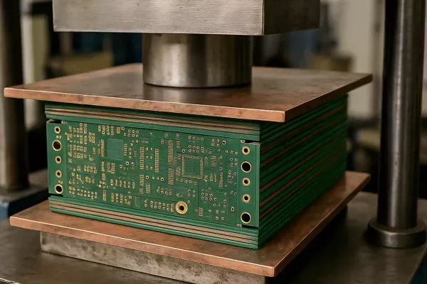
Misconception 4: Manufacturing Halogen-Free PCBs Is Far More Complex and Defect-Prone
Some view halogen-free production as requiring entirely new equipment or processes, increasing defect risks like warpage or poor adhesion. In practice, standard multilayer presses and drills handle these materials with minor parameter tweaks, such as slower ramp rates in lamination. Solder mask formulations must match to avoid compatibility issues, but once qualified, yields align with conventional runs. IPC standards guide inspection for surface quality and plating uniformity. Factories report consistent throughput after initial process validation.
Misconception 5: Halogen-Free PCBs Compromise Electrical Performance and Solderability
Engineers sometimes worry about degraded dielectric properties or solder joint integrity due to altered chemistry. Halogen-free dielectrics often provide superior insulation resistance from reduced polarity, benefiting high-speed signals. Solderability remains strong with immersion tin or ENIG finishes, as flux activation adapts to the surface energy. Assembly trials confirm reflow profiles transfer directly, minimizing defects like bridging. Performance of halogen-free PCBs meets or exceeds requirements in dense, fine-pitch designs.
Related Reading: Halogen-Free PCBs: What Engineers Need to Know
Practical Best Practices for Halogen-Free PCB Manufacturing
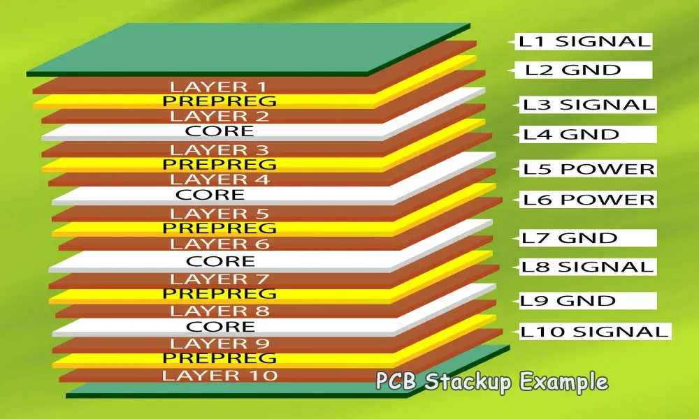
Selecting certified halogen-free laminates per IPC-4101B ensures traceability from the outset. Design stackups with balanced symmetry to mitigate warpage, targeting copper weights under 2 oz/ft2 for multilayer builds. Implement dry storage protocols, baking boards at 125°C for 24 hours before assembly to achieve MSL compliance. Validate solder processes with profilometers to confirm peak temperatures align with JEDEC guidelines. Collaborate with manufacturers on DfM reviews to address potential resin flow differences early. These steps integrate seamlessly into existing workflows, maximizing the advantages of halogen-free PCBs.
Related Reading: Halogen Free PCB Assembly: Best Practices for a Seamless Transition
Conclusion
Debunking halogen-free PCB misconceptions reveals these materials as viable, high-performing options for modern electronics. From cost considerations to thermal and electrical reliability, factory-driven insights confirm their parity with traditional alternatives. By aligning with standards like IPC and JEDEC, engineers can leverage environmental benefits without performance trade-offs. As adoption grows, the cost of halogen-free PCBs continues to normalize, making them a strategic choice for sustainable manufacturing.
FAQs
Q1: What are the main halogen-free PCB myths surrounding cost?
A1: Halogen-free PCB myths often exaggerate cost premiums, but material prices have stabilized with increased supply. Factory optimizations like standard tooling reduce overall expenses. Long-term savings from regulatory compliance and safer disposal outweigh initial differences. Engineers should request volume quotes for accurate comparisons.
Q2: Do halogen-free PCBs have performance drawbacks?
A2: Performance of halogen-free PCBs matches conventional boards in Tg, CTE, and signal integrity. Phosphorus-based resins enhance insulation while meeting IPC thermal qualifications. Minor process adjustments ensure assembly success. They excel in applications demanding low moisture sensitivity.
Q3: How does manufacturing differ for halogen-free boards?
A3: Manufacturing requires calibrated lamination and baking but uses standard equipment. JEDEC MSL handling prevents issues. Yields improve with qualified fluxes. No major complexity arises for experienced factories.
Q4: Why choose advantages of halogen-free PCBs over traditional ones?
A4: Advantages of halogen-free PCBs include reduced toxic fumes, better recyclability, and compliance. They offer lower absorption for humid conditions. Electrical properties support high-density designs effectively.
References
IPC-4101B — Specification for Base Materials for Rigid and Multilayer Printed Boards. IPC, 2006
IPC-6012E — Qualification and Performance Specification for Rigid Printed Boards. IPC, 2015
JEDEC J-STD-020E — Moisture/Reflow Sensitivity Classification for Nonhermetic Surface Mount Devices. JEDEC, 2014
JEDEC J-STD-609A — Marking and Labeling of Components, PCBs, and Passive Devices for Lead-Free and Halogen-Free Compliance. JEDEC, 2016