ALLPCB


Introduction
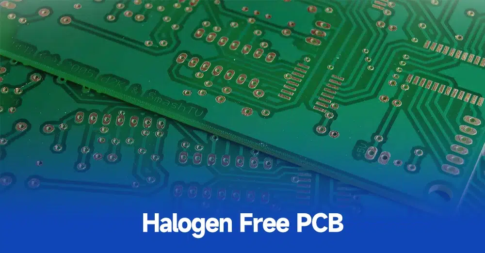
Transitioning to halogen-free PCB assembly represents a critical step for electronics manufacturers aiming to meet environmental regulations and enhance product safety. Halogen-free materials eliminate bromine and chlorine compounds traditionally used as flame retardants, reducing toxic emissions during recycling or fire events. Electric engineers must navigate unique challenges in the halogen-free PCB assembly process, including altered thermal behaviors and compatibility issues with existing workflows. This article outlines practical best practices to ensure reliable assembly outcomes. By focusing on material handling, process optimization, and troubleshooting, teams can achieve high yields without compromising performance. Understanding these elements allows for a smoother shift while maintaining assembly integrity.
What Is Halogen-Free PCB Assembly and Why Does It Matter?
Halogen-free PCB assembly involves soldering components onto printed circuit boards made from laminates with less than 900 parts per million of chlorine or bromine, and total halogens below 1500 parts per million. These boards use alternative flame retardants like phosphorus or nitrogen compounds to achieve similar fire resistance without hazardous halogens. The process aligns with global sustainability goals, as halogens can release corrosive gases when burned, posing risks in enclosed spaces like data centers or automotive modules.
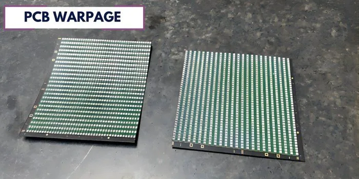
For electric engineers, the relevance lies in balancing eco-compliance with reliability under lead-free solder conditions. Traditional halogenated boards offer predictable thermal expansion, but halogen-free variants often exhibit higher moisture absorption and coefficient of thermal expansion (CTE), leading to potential warpage during reflow. Industry standards like IPC-4101 define specifications for these base materials, ensuring consistency across suppliers. Adopting halogen-free assembly future-proofs designs against tightening regulations while supporting recyclability.
Key Technical Challenges in Halogen-Free PCB Assembly
Halogen-free laminates typically feature higher glass transition temperatures (Tg) to withstand lead-free solder reflow peaks around 260 degrees Celsius, yet they decompose at lower temperatures than brominated alternatives. This creates a narrow process window where insufficient preheat can cause delamination, while excessive heat induces warpage. Moisture sensitivity classification per JEDEC J-STD-020 becomes crucial, as these materials absorb more humidity, risking voids or popcorning during soldering.
Component compatibility adds complexity, as mismatched CTE between board and parts can stress solder joints, especially with fine-pitch devices. Solder mask formulations must also be halogen-free to avoid contamination, influencing stencil release and paste adhesion. Warpage control demands symmetric stackups and fixturing, as asymmetric copper distribution amplifies bowing under thermal ramps. Engineers must profile reflow ovens meticulously to mitigate these interactions.
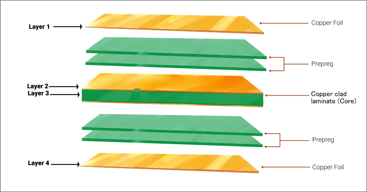
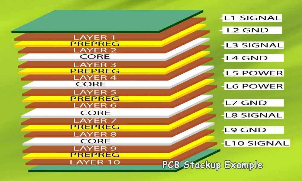
Best Practices for Material Selection and Preparation
Start with selecting high-Tg halogen-free laminates certified to IPC-4101, verifying solder mask and surface finishes for full compliance. Pre-bake boards at 125 degrees Celsius for four hours minimum to drive off absorbed moisture, extending beyond standard IPC Class 2 requirements for high-reliability apps. Store assemblies in dry nitrogen cabinets to prevent re-absorption, monitoring humidity below five percent relative.
Panelize designs with balanced copper distribution to minimize warpage, incorporating fiducials for precise alignment. Use lead-free compatible fluxes that avoid aggressive activators, pairing them with no-clean pastes for residue-free joints. Document material declarations from suppliers to trace halogen content throughout the supply chain. These steps establish a robust foundation for the halogen-free PCB assembly process.
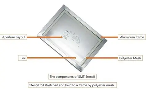
Optimizing Stencil Design for Halogen-Free Assemblies
Stencil design plays a pivotal role in achieving uniform solder paste deposition on halogen-free boards, where surface energy differs from traditional FR-4. Opt for electroformed or laser-cut stencils with 100 to 125 micron thickness to balance volume control and release properties. Reduce aperture walls by five to ten percent for fine-pitch components, preventing bridging while accommodating paste tackiness.
Incorporate step-down apertures for QFNs and BGAs, ensuring 75 percent paste coverage to compensate for potential voiding. Validate designs via solder paste inspection (SPI) post-printing, targeting volume tolerances within ten percent. Clean stencils with halogen-free solvents to avoid residue buildup, extending usability across runs. Proper stencil design enhances first-pass yields in lead-free solder applications.
Related Reading: Solder Paste Stencil Design: Key Factors for Perfect PCB Printing
Lead-Free Solder Paste Selection and Printing
Choose lead-free solder pastes with SAC305 alloys (96.5% tin, 3% silver, 0.5% copper) formulated for halogen-free compatibility, emphasizing low voiding and high slump resistance. Halogen-free fluxes rely on organic acids for activation, requiring precise printing parameters like 20 to 40 second snap-off times. Maintain stencil/printer gap at 1.27 millimeters and shear speeds around 20 to 50 millimeters per second for optimal transfer efficiency.
Inspect paste height uniformity across the board, adjusting pressure to 2 to 6 kilograms per square centimeter. Avoid overprinting, as excess paste exacerbates tombstoning on warpage-prone halogen-free surfaces. These practices ensure reliable joints without halide corrosion risks.
Reflow Profiling for Halogen-Free PCB Assembly
Reflow profiling demands a tailored curve for lead-free solder on halogen-free boards, starting with a linear preheat ramp of 1 to 3 degrees Celsius per second up to 150 degrees Celsius. Hold soak at 150 to 180 degrees Celsius for 60 to 120 seconds to activate flux evenly, minimizing defects like head-in-pillow. Peak above 240 degrees Celsius for 45 to 90 seconds ensures full melting without overheating the laminate.
Cool-down at 2 to 4 degrees Celsius per second prevents thermal shock, using nitrogen atmospheres to reduce oxidation. Profile multiple boards with thermocouples at corners and center, validating against IPC-6012 performance specs. Iterative tuning resolves hot spots, boosting joint integrity.
Related Reading: Halogen-Free PCBs: What Engineers Need to Know
Ensuring Component Compatibility and Placement
Verify component compatibility by matching lead-free plating (matte tin or ENIG) with halogen-free board finishes, avoiding nickel migration issues. Select MSL-rated parts per JEDEC J-STD-020, baking them alongside boards if needed. Use high-speed placers with vision systems to handle warpage, applying downward force on large BGAs.
For mixed-technology boards, sequence placement to prioritize sensitive passives before heavy connectors. Post-placement AOI checks alignment tolerances under 25 microns. This approach minimizes lift-offs and open joints.
Inspection and Rework Strategies
Post-reflow, employ automated X-ray for BGA voids and 3D AOI for solder fillet analysis, targeting zero bridging. Measure warpage with shadow moire interferometry, keeping below 0.75% for assemblies. Rework using conduction tools with localized preheat, adhering to hot air limits to preserve laminate integrity.
Document defects for root-cause analysis, adjusting profiles iteratively. These troubleshooting-focused inspections maintain quality in high-volume halogen-free runs.
Conclusion
Mastering halogen-free PCB assembly requires integrating best practices across material prep, stencil design, reflow profiling, and component compatibility. Electric engineers benefit from proactive warpage mitigation and precise process controls using lead-free solder. Standards like IPC-4101 and JEDEC J-STD-020 guide reliable transitions. Implementing these strategies yields robust, eco-friendly assemblies with minimal defects. Teams achieve seamless shifts by prioritizing data-driven optimizations and thorough validation.
FAQs
Q1: What are the main steps in the halogen-free PCB assembly process?
A1: The halogen-free PCB assembly process begins with moisture baking and stencil printing, followed by precise component placement and lead-free solder reflow. Key is optimizing reflow profiling to handle higher CTE and warpage risks. Post-reflow inspection via AOI and X-ray ensures joint quality. Troubleshooting focuses on flux compatibility and symmetric designs for yields above 99%.
Q2: How does stencil design impact halogen-free PCB assembly?
A2: Stencil design in halogen-free PCB assembly must account for altered surface tension, using thinner foils and reduced apertures for fine-pitch parts. This prevents bridging and ensures 75% paste volume on pads. Validate with SPI to catch inconsistencies early. Pairing with lead-free paste enhances release and minimizes voids during reflow.
Q3: Why is reflow profiling critical for component compatibility in halogen-free boards?
A3: Reflow profiling ensures component compatibility by providing even heating, avoiding thermal stress on halogen-free laminates with lead-free solder. Soak phases activate flux without delamination, while controlled peaks achieve liquidus. Nitrogen use reduces oxidation for sensitive parts. Profiles tuned per board size prevent warpage-induced offsets.
Q4: What precautions ensure lead-free solder success on halogen-free PCBs?
A4: Select SAC alloys with halogen-free fluxes, pre-bake materials per JEDEC J-STD-020, and use nitrogen reflow. Monitor warpage and adjust fixturing for flatness. Component leads must match finishes like ENIG. These steps mitigate voids and ensure reliable joints.