 ALLPCB


The True Cost of Trace Width and Spacing: Impact on PCB Component Pricing
Trace width and spacing directly influence the manufacturing processes required to produce a printed circuit board. Narrower traces and tighter spacing demand higher precision equipment and tighter process controls, which raise production expenses. These costs ultimately appear in the final component pricing passed along to design teams and procurement groups. Engineers who understand this relationship can make informed decisions during the layout phase that balance performance needs with budget constraints.
Why Trace Width and Spacing Affect PCB Economics
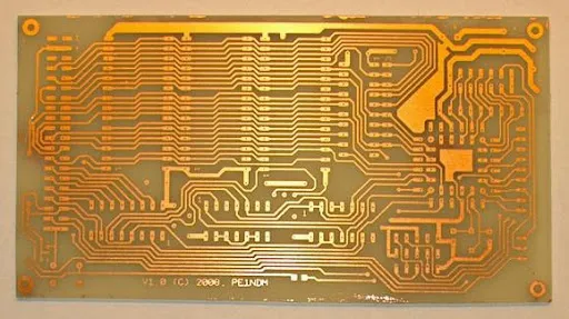
In high-density interconnect designs, trace width and spacing determine how many conductors fit within a given board area. Standard fabrication lines handle 6 mil or wider traces with conventional etching chemistry and standard photoresist materials. When designers specify 3 mil or finer features, fabricators must switch to advanced processes such as laser direct imaging, finer-grain copper foils, and controlled etch compensation. Each of these steps adds equipment time, consumable costs, and lower first-pass yields, all of which increase the per-panel price.
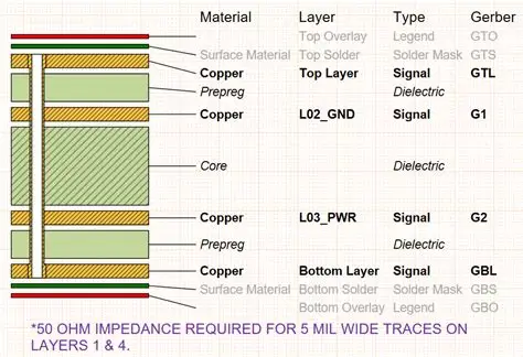
Impedance-controlled boards add another layer of cost sensitivity. Maintaining a target impedance often requires precise trace width and dielectric thickness combinations. Deviations caused by etching variation become unacceptable at fine geometries, forcing additional test coupons, impedance measurements, and potential panel scrapping. The cumulative effect appears in higher unit pricing, particularly for prototypes and low-to-medium volume runs where setup amortization is limited.
Engineering Mechanisms Behind Cost Escalation
Etching uniformity becomes critical once trace widths drop below 5 mil. Isotropic etch chemistry removes copper equally in all directions, so narrower lines suffer proportionally greater width reduction from side-wall attack. Fabricators compensate by starting with thicker copper or using more aggressive etch control, both of which raise material and process expenses. Yield loss from over-etch or under-etch further multiplies cost because each defective panel reduces the number of shippable boards per production lot.
Fine-line requirements also affect plating and surface-finish operations. Copper plating thickness must remain consistent across narrow traces to avoid current-density crowding that produces dog-bone profiles. Achieving this uniformity often requires slower plating rates or pulse plating techniques, extending cycle time in the plating bath. Solder-mask application follows the same pattern: finer features demand higher-resolution masks and tighter registration tolerances, increasing both material cost and inspection time.
Thermal and mechanical stresses during lamination and reflow can exacerbate issues with dense trace patterns. Closely spaced traces increase the risk of copper migration or delamination if the resin system cannot fully encapsulate the conductors. IPC-6012E outlines the performance requirements that boards must meet, and finer geometries push fabricators closer to the edge of acceptable process windows, often necessitating more rigorous qualification testing.
Design Practices That Control Cost
Designers can minimize unnecessary cost by establishing clear trace-width rules early in the project. Using the widest trace that still satisfies current-carrying and impedance requirements reduces the need for advanced fabrication steps. Many boards achieve acceptable density with 5 mil or 6 mil traces when layer count or board size can be adjusted slightly. This approach avoids the steep cost curve associated with sub-4 mil features.
Design-for-manufacturing reviews should include a cost-impact assessment of trace and space specifications. Fabricators typically publish capability matrices that list standard, advanced, and premium pricing tiers based on minimum feature size. Aligning the layout to the standard tier whenever possible keeps the board within conventional process windows and preserves higher yields. When fine lines are unavoidable, spreading critical nets across multiple layers or using via-in-pad technology can sometimes relax the requirements on any single layer.
Material selection also plays a role. Higher-performance laminates with tighter thickness tolerances support finer geometries without additional process controls, yet they carry their own premium. Balancing laminate grade against trace-width demands often yields a lower total cost than pushing a standard material to its limit with ultra-fine features.
Practical Guidance for Engineers and Procurement
Procurement teams benefit from requesting multiple quotations that explicitly separate pricing by minimum trace and space. This transparency reveals how aggressively fine features drive cost and allows comparison of different design iterations. Early collaboration between layout engineers and the fabrication team can identify opportunities to relax non-critical areas while preserving performance in high-speed or high-current zones.
When impedance control is required, specifying only the nets that truly need tight tolerance avoids over-constraining the entire board. Many designs contain a mixture of controlled-impedance and non-controlled traces; segregating them reduces the percentage of the board that must undergo premium processing.
Conclusion
Trace width and spacing choices propagate through every stage of PCB fabrication and directly shape component pricing. Wider, standard geometries generally deliver lower cost and higher yield, while fine-line requirements trigger specialized equipment, tighter process controls, and increased inspection. Engineers who apply these principles during layout can achieve required electrical performance without incurring avoidable premiums. Clear communication of design intent and early DFM engagement remain the most effective tools for managing the true cost of trace and space decisions.
FAQs
Q1: How does PCB trace width cost change when moving from 6 mil to 3 mil features?
A1: Moving from 6 mil to 3 mil traces typically shifts fabrication from standard to advanced process tiers. This change increases the need for higher-resolution imaging, tighter etch control, and additional quality checks, resulting in higher per-unit pricing especially noticeable in smaller production volumes.
Q2: What role does fine-line PCB manufacturing cost play in overall board pricing?
A2: Fine-line PCB manufacturing cost becomes a significant portion of total board price once minimum trace and space fall below conventional capability limits. The added process steps, lower yields, and specialized materials compound to raise the final delivered cost to the customer.
Q3: How does impedance control and price interact with trace width selection?
A3: Impedance control and price are linked because achieving target impedance at fine trace widths demands tighter control of copper thickness and dielectric spacing. These tighter tolerances often require premium materials or extended process times, elevating the overall board price compared with non-controlled designs.
Q4: When should designers consider minimizing trace width for cost?
A4: Designers should evaluate minimizing trace width for cost whenever electrical requirements can be met with wider traces or additional layers. This approach keeps the design within standard fabrication capabilities and avoids the cost escalation associated with fine-line processing.
References
IPC-6012E — Qualification and Performance Specification for Rigid Printed Boards. IPC, 2017
IPC-A-600K — Acceptability of Printed Boards. IPC, 2020
IPC-2221B — Generic Standard on Printed Board Design. IPC, 2012


