 ALLPCB


Introduction
Flux plays a critical role in PCB wave soldering by enabling reliable solder joints through oxide removal and surface tension reduction. In the wave soldering process, PCBs travel through a fluxer, preheater, and solder wave, where flux activates to clean metal surfaces just before solder contact. Without proper flux, oxides on leads, pads, and solder form barriers that prevent wetting and lead to defects like bridging or incomplete fills. Engineers must select flux based on assembly requirements to balance performance, cleanliness, and reliability. This article explores PCB wave soldering flux types, application methods, residue management, and more, offering practical insights for optimizing wave soldering outcomes. Understanding these elements ensures compliance with industry standards and minimizes troubleshooting.
Understanding Flux in PCB Wave Soldering
Flux is a chemical agent that removes oxides, prevents reoxidation during heating, and promotes solder flow on PCB surfaces. In wave soldering, it temporarily protects bare copper or tinned leads from atmospheric oxygen while improving capillary action between components and pads. Common PCB wave soldering flux types include rosin-based, water-soluble, and no-clean varieties, each suited to different contamination levels and post-process needs. Rosin fluxes derive from natural pine resins and offer mild activity for clean assemblies, while water-soluble types use synthetic activators for heavily oxidized surfaces. No-clean fluxes leave benign residues that do not require removal in many cases, making them popular for high-volume production. J-STD-004 classifies these fluxes by composition and activity, guiding selection for consistent results.
The importance of flux stems from the high temperatures in wave soldering, typically around 250 degrees Celsius for solder, which accelerate oxidation without protection. Flux vehicles, often alcohols or glycols, evaporate during preheating to leave activators on the board. Poor flux choice leads to issues like solder balls, icicles, or dewetting, detectable under IPC-A-610 criteria for joint acceptability. Engineers troubleshoot by evaluating flux spread uniformity and preheat profiles to match flux activation. Proper flux ensures joints meet mechanical and electrical reliability standards across diverse PCB designs.
PCB Wave Soldering Flux Types and Activity Levels
PCB wave soldering flux types fall into categories defined by their base materials and performance characteristics. Rosin fluxes, labeled as R under J-STD-004, provide low to high activity with minimal corrosion risk when residues are managed. Organic fluxes, denoted OR, suit applications needing higher activity without halide content, while water-soluble fluxes, often WS or OR, excel on difficult surfaces but demand thorough cleaning. No-clean fluxes, typically ROL0 or REL0, minimize post-solder intervention by leaving non-conductive, non-corrosive residues. Activity levels range from L (low) for electronics with minimal oxides to H (high) for challenging metals, with sublevels 0 or 1 indicating halide presence.
Flux activity measures oxide removal and wetting promotion, directly impacting joint quality. Low-activity fluxes suffice for tinned components and clean HASL or ENIG finishes, reducing residue concerns. Medium-activity options balance performance for mixed assemblies, while high-activity fluxes tackle bare copper or OSP surfaces but risk corrosion if residues persist. Engineers assess activity via bell test corrodibility under J-STD-004, ensuring compatibility with class 2 or 3 products. Solid content, usually 2 to 5 percent, influences film thickness and bridging prevention. Selecting the right PCB wave soldering flux activity prevents defects while aligning with cleanliness goals.
Criteria for Selecting Wave Soldering Flux
Selection begins with PCB finish, component lead types, and process class per J-STD-001 soldering requirements. For lead-free assemblies, fluxes must withstand higher temperatures without excessive fuming or splattering. Board density dictates flux type; high-component-count boards favor low-residue no-clean to avoid bridging under shadows. Environmental factors like humidity influence hygroscopic residues, prompting low-solid-content choices. Test flux on sample panels for wetting angle and residue SIR (surface insulation resistance) to predict field performance.
Practical considerations include machine compatibility and throughput. Foaming fluxes suit turbulent waves, while spray fluxes offer precision for fine-pitch. Cost-effectiveness weighs cleaning needs against defect rates; water-soluble fluxes cut initial defects but add wash steps. Engineers prototype with flux qualifiers, monitoring solderability via meniscus height tests. Alternatives like low-solids formulations reduce flux consumption by 20 to 30 percent in optimized lines. Always verify flux shelf life and storage to maintain efficacy.
PCB Wave Soldering Flux Application Methods
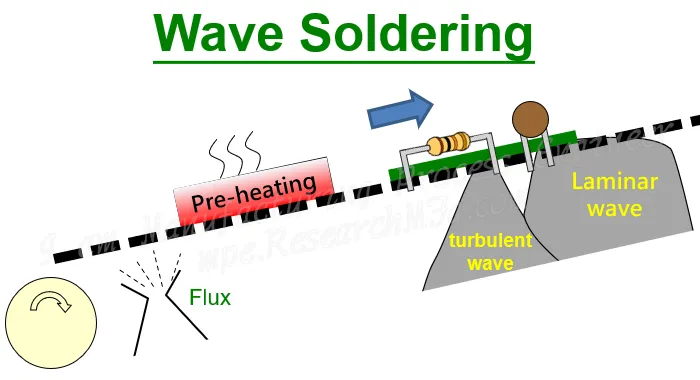
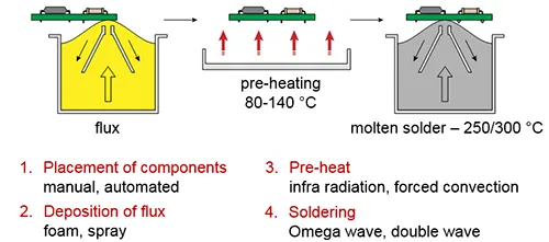
PCB wave soldering flux application methods include spray, foam, and drop-jet systems, each optimizing coverage and minimizing excess. Spray fluxers use nozzles to atomize flux into a uniform mist, ideal for double-sided boards needing top and bottom coverage. Foam methods bubble flux through a block to create gentle froth, reducing overspray and suited for selective wetting on through-hole components. Drop-jet or micro-spray variants deposit precise droplets, preventing flux shadows on dense BGAs or QFPs.
Application timing aligns with conveyor speed and preheat zone entry, ensuring flux dries partially before solder contact. Flux volume, controlled at 500 to 2000 micrograms per square centimeter, prevents drowning pallets or components. Troubleshooting uneven application involves nozzle alignment and pressure checks, often revealed by flux pooling under IPC-A-610 inspection. Preheat temperatures, around 100 to 150 degrees Celsius, activate flux without boiling solvents prematurely.
Wave height and angle further interact with flux; turbulent waves demand higher-activity formulations for penetration. Maintenance like daily fluxer rinses prevents contamination buildup. Engineers log application parameters for process control charts, correlating to first-pass yields.
Managing PCB Wave Soldering Flux Residues
Post-soldering, flux residues can cause electromigration or dendritic growth if conductive or hygroscopic. No-clean residues, designed per J-STD-004 as L0 or M0, pass SIR tests above 100 megaohms, allowing omission of cleaning in class 2 assemblies. Water-soluble residues, however, hydrolyze into corrosives, necessitating immediate deionized water rinses at 40 to 60 degrees Celsius. Ultrasonic or spray-in-air washers remove 95 percent of residues, verified by ion chromatography for halides below 2 micrograms per square centimeter.
Residue removal starts with in-line defluxing post-wave, using heated DI water cascades followed by hot air drying. For no-clean, optional IPA vapor or solvent wipes address visible white residue from rosin flux. Visual inspection under black light reveals incomplete cleaning, guiding adjustments. Engineers prioritize residue-free zones near high-voltage traces or connectors.
Troubleshooting persistent residues involves flux dilution checks and washer filtration. Over time, residue accumulation signals fluxer drift or preheat shortfalls.
PCB Wave Soldering Flux Alternatives and Innovations
While traditional liquid fluxes dominate, PCB wave soldering flux alternatives include nitrogen blanketing to suppress oxidation, reducing flux needs by half. Low-flux or fluxless soldering uses formic acid vapors for oxide reduction, viable for simple through-hole boards. Plasma cleaning pre-treats surfaces for oxide-free starts, pairing with minimal flux sprays.
Selective soldering machines apply flux only to targeted joints, cutting overall usage. Emerging synthetic fluxes with polymer vehicles offer zero-residue profiles, though compatibility testing remains essential. Engineers evaluate alternatives via DOE (design of experiments) for cost-yield tradeoffs. Hybrid approaches, like nitrogen plus low-activity flux, optimize for lead-free high-Tg boards.
Best Practices and Troubleshooting
Implement flux management with daily SIR testing and flux bath analysis for solids and pH. Standardize preheat profiles to match flux activation curves, avoiding cold spots. Train operators on fluxer height adjustments for pallet types. Common defects like solder balls trace to overfluxing; reduce by 10 percent increments.
For bridging, increase drop size or switch to medium-activity. Dewetting signals insufficient activity; test higher levels cautiously. Document SPC data linking flux parameters to AQL rejects. Periodic audits per IPC-A-610 ensure class compliance.
Conclusion
Flux remains indispensable in PCB wave soldering, with selection, application, and residue control dictating joint integrity. Mastering PCB wave soldering flux types, activity levels, and methods empowers engineers to achieve high yields. Residue removal safeguards long-term reliability, while alternatives expand options for challenging designs. Adhering to standards like J-STD-004 and J-STD-001 minimizes risks and supports scalable production. Prioritize testing and process discipline for optimal results.
FAQs
Q1: What are the main PCB wave soldering flux types?
A1: Rosin-based (R), organic (OR), and water-soluble (WS) fluxes represent primary types, classified under J-STD-004. Rosin offers mild activity for clean boards, organics balance performance without halides, and WS handles heavy oxides but requires cleaning. Selection depends on surface finish and class requirements, with no-clean variants popular for efficiency. Activity levels from L to H guide choices for wetting reliability.
Q2: How do PCB wave soldering flux application methods differ?
A2: Spray provides uniform mist for broad coverage, foam generates gentle froth to minimize excess, and drop-jet targets precise areas. Spray suits high-volume lines, foam reduces bridging on dense boards, and drop-jet excels in selective processes. Conveyor speed and flux volume control thickness, with preheat ensuring activation. Method choice impacts throughput and defect rates.
Q3: What are effective PCB wave soldering flux residue removal techniques?
A3: Deionized water spray or ultrasonic cleaning removes water-soluble residues effectively, followed by drying. No-clean types often need no action if SIR-tested, but IPA swabbing clears visible buildup. Ion testing verifies cleanliness below critical thresholds. Timing post-wave prevents corrosion, with in-line systems preferred for volume.
Q4: What PCB wave soldering flux alternatives exist?
A4: Nitrogen atmospheres reduce oxidation needs, fluxless formic processes suit simple joints, and plasma preps enable low-flux use. Hybrids combine minimal flux with inert gas for lead-free. Testing ensures joint quality matches traditional methods. Alternatives lower costs but demand process tweaks.
References
J-STD-004 — Requirements for Soldering Fluxes. IPC/JEDEC
J-STD-001 — Requirements for Soldered Electrical and Electronic Assemblies. IPC, 2017
IPC-A-610 — Acceptability of Electronic Assemblies. IPC


