ALLPCB


High-density interconnect printed circuit boards enable compact, high-performance electronic systems used in telecommunications, automotive electronics, and medical devices. Design for manufacturability plays a central role in ensuring these boards can be produced reliably at scale while meeting performance targets. Industry standards provide the framework that guides engineers through layout decisions, material selections, and process controls. When followed consistently, these standards reduce the risk of defects such as trace opens, via failures, and registration errors that commonly arise in dense designs. Effective application of PCB design standards DFM therefore supports both product quality and production efficiency.
Why IPC Standards Matter for HDI Boards
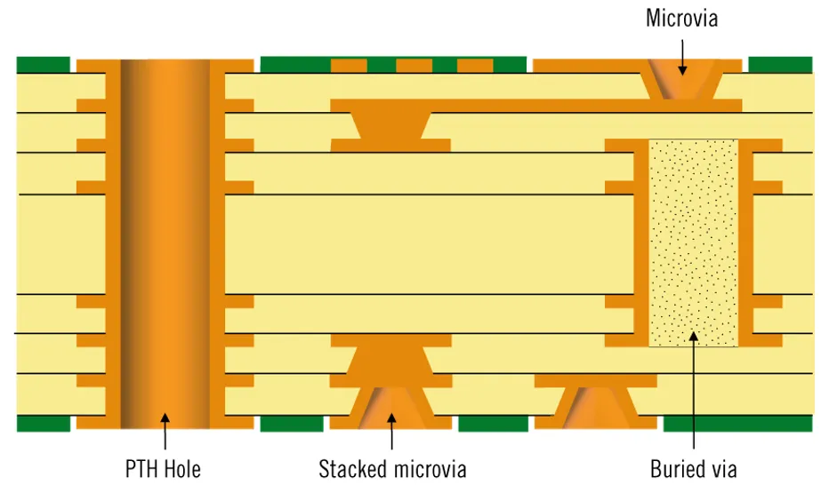
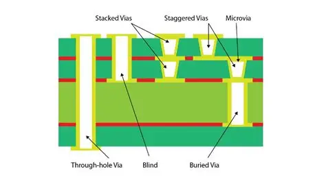
High-density interconnect technology relies on fine lines, small vias, and multiple build-up layers to achieve greater functionality within limited board area. Without clear guidelines, designers may create layouts that exceed fabrication capabilities or introduce reliability risks during assembly and operation. IPC-2221 establishes foundational requirements for printed board design that apply across many product classes. These requirements help teams balance electrical performance, thermal management, and mechanical stability from the earliest stages of development. When combined with HDI-specific considerations, the standards promote designs that align with available manufacturing processes and inspection methods.
Technical Principles Guiding DFM Decisions
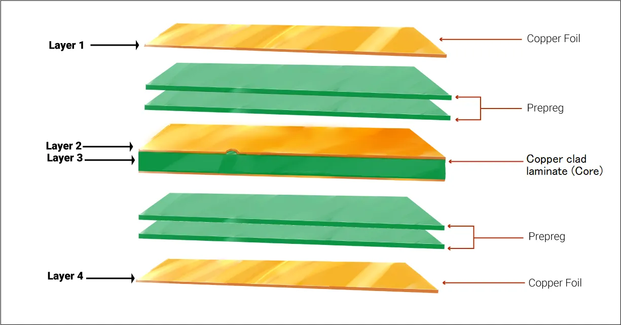
IPC-2226 HDI standards define sectional requirements for high-density interconnect printed boards, including conductor spacing, via structures, and layer registration tolerances. These specifications address the unique challenges of sequential lamination and microvia formation that distinguish HDI from conventional multilayer boards. Engineers apply the principles by calculating minimum feature sizes based on the selected fabrication process and by planning stack-ups that maintain adequate dielectric spacing. Thermal expansion differences between materials must also be considered to prevent warpage or delamination during reflow. The result is a design that remains manufacturable while preserving signal integrity and power distribution performance.

IPC-6012 Class 3 defines qualification and performance criteria for rigid printed boards intended for high-reliability applications. Class 3 boards undergo more stringent testing for plating thickness, hole quality, and surface finish integrity than lower classes. Designers incorporate these expectations by specifying appropriate copper weights, via fill methods, and surface treatments early in the layout phase. This approach minimizes the need for design revisions after prototype fabrication and supports consistent yields during volume production. The standards therefore serve as a common reference that aligns design intent with manufacturing verification.
Practical Implementation in Design and Production
Design teams begin by reviewing the target product class and reliability requirements against the relevant IPC documents. They then establish design rules that incorporate minimum trace widths, annular ring dimensions, and via aspect ratios consistent with those documents. Collaboration between layout engineers and manufacturing partners helps identify potential conflicts before artwork release. Simulation tools can further validate thermal and electrical performance under the constraints defined by the standards. Regular design reviews that reference the same criteria reduce iteration cycles and support smoother transition to fabrication.
During manufacturing, process controls focus on maintaining registration accuracy across build-up layers and ensuring microvia plating quality. Inspection protocols aligned with the standards verify conductor integrity and dielectric spacing before proceeding to subsequent operations. When deviations occur, root-cause analysis often traces back to design choices that approached the limits of the specified tolerances. Adjusting those choices in subsequent revisions improves overall process capability and reduces scrap rates.
Best Practices for Sustained Compliance
Engineers maintain a living set of design rules derived directly from the applicable IPC sections and update them as new revisions are released. Documentation of material selections, stack-up details, and via constructions provides traceability that supports both internal audits and customer qualification. Training programs ensure that all team members interpret the standards consistently, avoiding subjective variations that can lead to quality escapes. When new HDI features such as any-layer vias or filled microvias are introduced, teams perform capability studies to confirm that the chosen processes remain within the standard limits. This disciplined approach embeds DFM into the development workflow rather than treating it as a final checklist item.

Conclusion
IPC standards supply the technical foundation that enables reliable design and manufacture of high-density interconnect boards. By integrating the requirements of IPC-2221, IPC-2226 HDI standards, and IPC-6012 Class 3 into daily workflows, engineering teams achieve better alignment between design intent and production reality. The outcome is fewer late-stage changes, improved first-pass yields, and products that meet the demanding expectations of modern electronics applications. Consistent application of these guidelines continues to support innovation while preserving the manufacturability and reliability essential for long-term success.
FAQs
Q1: How do IPC-2221 and IPC-2226 HDI standards influence trace and via design rules in high-density PCBs?
A1: These standards establish minimum dimensions and spacing requirements that account for fabrication process capabilities and long-term reliability. Designers use the specified values to set layout constraints that prevent common defects such as insufficient annular rings or excessive aspect ratios. Following the guidelines early in the project reduces the likelihood of manufacturing issues and supports consistent electrical performance across production lots.
Q2: What role does IPC-6012 Class 3 play in DFM for high-reliability HDI boards?
A2: IPC-6012 Class 3 defines acceptance criteria for plating, hole quality, and overall board construction that exceed those of lower classes. Incorporating these criteria during layout helps ensure the finished product can pass qualification testing without requiring redesign. The standard therefore guides material and process selections that align with the performance needs of critical applications.
Q3: How can teams ensure HDI manufacturing guidelines are followed throughout the development cycle?
A3: Teams integrate the relevant sections of the standards into their design rule sets and conduct regular reviews with manufacturing partners. Documentation of stack-ups, via structures, and material properties provides a clear reference for all stakeholders. Capability studies and process audits further confirm that production remains within the defined limits, supporting repeatable results from prototype through volume manufacturing.
Q4: What are common DFM challenges when applying PCB design standards to dense interconnect layouts?
A4: Challenges often arise from attempting feature sizes or via configurations that approach or exceed the limits outlined in the standards. Insufficient planning for layer registration or thermal expansion can also create issues during sequential lamination. Addressing these factors through early collaboration and simulation helps maintain compliance while achieving the desired board density and functionality.