 ALLPCB


Introduction
In high-speed PCB designs, precise PCB impedance control is essential to maintain signal integrity and minimize reflections. Copper cladding, referring to the copper foil layers laminated onto the dielectric substrate, plays a subtle yet critical role in this process. Variations in copper thickness and surface characteristics directly influence the characteristic impedance of transmission lines. Engineers must account for these factors during stackup design to ensure consistent performance across microstrip and stripline structures. This article explores how controlled impedance copper cladding affects overall PCB performance, drawing on established engineering principles. Understanding these interactions helps optimize designs for reliable operation in demanding applications.
Understanding Copper Cladding and Its Role in PCBs
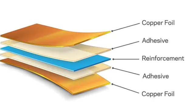
Copper cladding forms the foundational conductive layers in printed circuit boards, typically applied as thin foils to both sides of a dielectric core. Standard weights range from 0.5 oz per square foot to 3 oz, corresponding to thicknesses of approximately 18 micrometers to 105 micrometers before processing. During manufacturing, outer layer copper thickens due to plating, which alters the final dimensions used in impedance calculations. The type of copper foil, such as electrodeposited or rolled annealed, also impacts adhesion, roughness, and electrical properties. In the context of PCB impedance control, copper cladding ensures uniform current distribution and reference planes for controlled transmission lines. Proper selection prevents deviations that could degrade signal quality.
Why PCB Impedance Control Matters in Modern Designs
High-frequency signals propagate as transmission lines on PCBs, where mismatches in characteristic impedance lead to reflections, crosstalk, and data errors. Controlled impedance copper cladding enables designers to match trace geometry with dielectric properties for target values like 50 ohms or 100 ohms differential. This is particularly vital in multilayer boards with dense routing. Microstrip impedance and stripline impedance require precise stackup definitions to account for all variables. Without tight control, even small variations amplify losses at gigahertz frequencies. Industry practices emphasize impedance as a key metric for signal integrity verification.
Technical Principles: Copper Cladding's Influence on Impedance
Characteristic impedance derives from the inductance and capacitance per unit length of a transmission line, governed by geometry and materials. In microstrip structures, the signal trace sits atop a dielectric with a ground plane below, exposing part of the field to air. Copper thickness impedance becomes a factor here, as thicker foil effectively widens the conductor, reducing impedance slightly for fixed trace width and height. Formulas used in design incorporate copper thickness t alongside trace width w, dielectric height h, and relative permittivity Er. For instance, increased t lowers Z0 by enhancing capacitance through better field confinement. Surface roughness of the copper cladding further modulates effective permittivity at high frequencies due to skin effect.
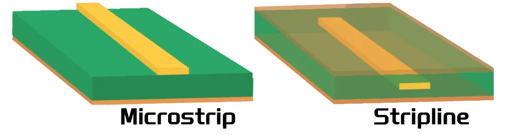
Stripline configurations embed the trace between two ground planes, offering better shielding but demanding symmetric dielectrics. Here, copper thickness impedance effects are similar but compounded by dual reference planes, making stackup uniformity critical. As per IPC-2141A guidelines, designers must model both inner and outer layer copper weights accurately. Plating on outer layers can increase thickness by 20 to 50 percent, necessitating adjustments in trace widths to maintain target impedance. Copper foil profile, such as low-profile versus standard, influences loss tangent and insertion loss independently of DC thickness. These principles underscore why controlled impedance copper cladding demands precise specification from layout to fabrication.
Key Factors Affected by Copper Cladding in Impedance Control
Dielectric thickness dominates impedance variation, but copper cladding contributes through dimensional tolerances and processing. Manufacturing tolerances on foil thickness typically hold at ±10 percent, yet plating buildup on signal layers requires compensation. In microstrip impedance calculations, neglecting copper thickness leads to 2 to 5 percent errors in predicted Z0. For stripline impedance, inner layer etch-back during lamination slightly thins copper, altering field distribution. Reference plane copper weight must match signal layers for balanced coupling. Additionally, copper roughness increases effective path length for AC currents, degrading impedance control above 1 GHz.
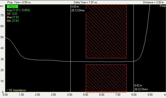
Environmental factors like temperature affect copper resistivity, indirectly influencing impedance over time. IPC-2221A outlines design rules for conductor sizing that integrate these considerations. Engineers use field-solving software to simulate full stackups, inputting exact copper parameters. Validation via time-domain reflectometry confirms fabricated impedances within ±10 percent tolerance. These interconnected factors highlight copper cladding's foundational role in robust PCB impedance control.
Best Practices for Achieving Controlled Impedance with Copper Cladding
Start with a symmetric stackup to minimize warpage and ensure uniform dielectric spacing around traces. Specify copper weights explicitly in fabrication notes, distinguishing starting and finished thicknesses. For high-speed designs, opt for low-roughness copper foils to preserve microstrip impedance at elevated frequencies. Adjust trace widths iteratively using impedance calculators that include copper thickness impedance effects. Maintain consistent copper density across layers to avoid localized etching variations that skew impedance.
Collaborate early with fabricators to align on process capabilities, such as panel plating versus pattern plating. IPC-2141A recommends tolerance bands like ±5 ohms for critical nets. Perform pre-layout simulations and post-etch TDR testing on coupons. Document stackup details thoroughly, including foil types and plating additions. These steps ensure controlled impedance copper cladding translates to production reality.
Troubleshooting Common Issues with Copper Cladding and Impedance
Impedance deviations often stem from unaccounted plating thickness on outer layers, causing lower-than-expected Z0 in microstrip lines. Verify stackup drawings against as-built cross-sections to identify discrepancies. Excessive copper roughness manifests as increased insertion loss without DC resistance changes. Switch to reverse-treated foil for better high-frequency performance. Asymmetric lamination in striplines leads to mode conversion; resolve with balanced prepreg selection.
Fabrication-induced etch variations amplify copper thickness impedance sensitivity in fine-pitch designs. Implement test coupons at board edges for inline TDR checks. If warpage distorts dielectric heights, reinforce with heavier inner copper planes. Systematic root-cause analysis, guided by standards like IPC-6012E, resolves most issues efficiently.
Conclusion
Copper cladding profoundly shapes PCB impedance control through its thickness, profile, and processing interactions. Mastering microstrip impedance and stripline impedance requires integrating these elements into stackup and routing strategies. Adhering to best practices ensures signal integrity in high-speed applications. Engineers benefit from precise modeling and verification to harness controlled impedance copper cladding effectively. Ultimately, thoughtful design yields reliable, high-performance boards ready for demanding environments.
FAQs
Q1: How does copper thickness affect PCB impedance control?
A1: Copper thickness impedance influences characteristic impedance by altering effective conductor width and capacitance in transmission lines. Thicker copper slightly lowers Z0 for fixed geometry in both microstrip and stripline setups. Designers compensate by widening traces during layout. Manufacturing plating adds to outer layer thickness, requiring precise stackup specs. This ensures controlled impedance copper cladding meets target values within tolerance.
Q2: What is the difference in copper cladding impact on microstrip impedance versus stripline impedance?
A2: Microstrip impedance exposes fields to air, making copper thickness more pronounced due to partial fringing. Stripline impedance benefits from enclosed fields between planes, with copper effects more uniform but sensitive to etch-back. Both demand accurate modeling per IPC-2141A. Controlled impedance copper cladding optimizes both for minimal reflections.
Q3: Why is controlled impedance copper cladding important for high-speed PCBs?
A3: Controlled impedance copper cladding prevents signal reflections by matching trace Z0 to driver and receiver specs. Variations from foil thickness degrade eye diagrams and bit error rates. It supports dense routing without crosstalk. Proper selection enhances overall PCB impedance control reliability.
Q4: How can engineers optimize copper thickness for impedance control?
A4: Select foil weights based on current needs while simulating impedance impacts. Account for 25 to 50 micrometer plating buildup on signals. Use low-profile copper for GHz signals. Validate with TDR on prototypes. This approach refines PCB impedance control effectively.
References
IPC-2141A — Design Guide for High-Speed Controlled Impedance Circuit Boards. IPC, 2004
IPC-2221A — Generic Standard on Printed Board Design. IPC, 2003
IPC-6012E — Qualification and Performance Specification for Rigid Printed Boards. IPC, 2017


