 ALLPCB


Introduction
Immersion tin serves as a popular lead-free surface finish for printed circuit boards, providing excellent initial solderability and a flat surface ideal for fine-pitch components. During surface mount technology assembly, reflow soldering exposes the immersion tin layer to high temperatures, triggering reactions that form intermetallic compounds at the copper-tin interface. These intermetallic compounds, or IMCs, play a critical role in joint integrity but can also lead to challenges like reduced solderability after reflow if not managed properly. Electric engineers must grasp how immersion tin reflow soldering influences IMC formation to ensure reliable assemblies under thermal cycling conditions. This article explores the mechanisms, impacts, and practical strategies for optimizing performance. By understanding Cu3Sn and Cu6Sn5 growth, teams can troubleshoot issues and enhance long-term reliability.
What Is Immersion Tin and Why Does Reflow Soldering Matter?
Immersion tin involves a chemical displacement process where tin deposits directly onto exposed copper pads, creating a thin, uniform layer that protects against oxidation. This finish excels in press-fit applications and multiple soldering steps due to its solder-wetting properties. Reflow soldering, the standard process for attaching components, melts solder paste in a controlled oven profile, typically peaking above 220°C for lead-free alloys. The interaction between molten solder, immersion tin, and underlying copper drives IMC formation, which bonds the joint but consumes the tin layer. For electric engineers, this matters because excessive IMC growth degrades solderability after reflow, leading to defects like de-wetting or voids. Standards like IPC-4554 outline requirements for immersion tin thickness and performance to guide these processes.
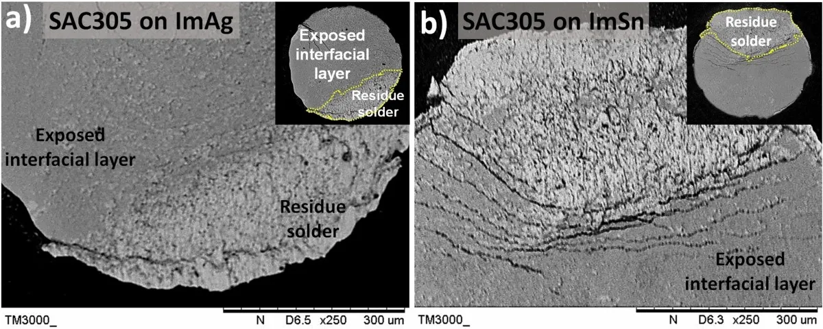
Mechanisms of IMC Formation during Immersion Tin Reflow Soldering
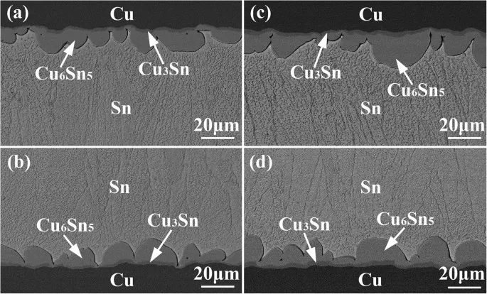
When the reflow temperature reaches the tin melting point around 232°C, the immersion tin layer dissolves into the molten solder, allowing copper atoms to diffuse upward. This rapid reaction primarily forms Cu6Sn5, a scallop-shaped intermetallic compound at the solder-interface, which provides a strong metallurgical bond. Cu3Sn develops more slowly at the copper-Cu6Sn5 boundary through solid-state diffusion, acting as a barrier that limits further copper migration. The first reflow cycle consumes a significant portion of the tin, converting it into these IMCs and leaving remnants on the surface. Subsequent cycles accelerate growth, as residual tin islands react further, thickening the IMC layer. Engineers observe this via cross-sectional analysis, where Cu6Sn5 dominates initially, transitioning to more Cu3Sn with prolonged exposure.
The diffusion kinetics follow parabolic growth laws, influenced by temperature, time above liquidus, and cooling rates. Higher peak temperatures promote faster Cu6Sn5 nucleation, while slower ramps allow Cu3Sn to thicken. In immersion tin reflow soldering, the thin tin deposit means full consumption occurs after just a few cycles, exposing brittle IMCs. This exposure alters surface energy, hindering fresh solder wetting. Practical microscopy reveals scalloped Cu6Sn5 morphology, which can trap flux residues if not optimized.
Impact of IMC Formation on Solderability after Reflow
Solderability after reflow declines as the pure tin depletes, replacing it with IMC-covered surfaces that exhibit poorer wetting. Cu6Sn5 offers decent solderability initially, but Cu3Sn, being more brittle and less wettable, dominates after multiple reflows, causing de-wetting defects. Engineers report non-wetting on pads where tin islands vanish, leading to tombstoning or bridging in assemblies. The IMC thickness correlates directly with reflow cycles; even three passes can expose enough Cu3Sn to fail wetting tests. Flux compatibility becomes crucial, as aggressive types etch IMCs unevenly, exacerbating issues. Troubleshooting involves zeroing in on reflow profiles to minimize time above 217°C, preserving tin for secondary operations.
Oxidation during air reflow further complicates matters, forming tin oxide that resists flux activation on IMC sites. Post-reflow inspection via dip-and-look simulates wave soldering, revealing dewetting percentages that spike with IMC exposure. For high-reliability boards, maintaining solderability after reflow demands precise process control. J-STD-020 guidelines for moisture and reflow sensitivity help classify boards, ensuring immersion tin withstands assembly stresses without delamination.
Effects of Thermal Cycling on IMC Growth and Joint Reliability
Thermal cycling simulates operational stresses, accelerating IMC growth through repeated expansion and contraction. Under cycles from -40°C to 125°C, Cu6Sn5 coarsens, while Cu3Sn thickens at grain boundaries, promoting cracks in the intermetallic layer. This spalling weakens the joint, as detached Cu6Sn5 particles migrate into the solder bulk. Immersion tin reflow soldering sets the baseline IMC thickness, which thermal cycling amplifies via diffusion-enhanced mechanisms. Engineers measure reliability via shear testing, where thicker IMCs reduce ductility, leading to fatigue failure. Voiding at the IMC-solder interface increases under cycling, driven by Kirkendall voids from unequal diffusion rates.
Long-term aging at elevated temperatures mirrors cycling effects, with Cu3Sn converting Cu6Sn5 over time. Practical data shows joints failing after 1000 cycles if initial reflow overgrows IMCs. Mitigation focuses on alloy selection and finish thickness per IPC-4554, balancing initial solderability with endurance. Cross-sectioning cycled samples reveals planar Cu3Sn layers exceeding 1 μm, correlating to 20% strength loss.

Best Practices and Troubleshooting for Immersion Tin Reflow Soldering
Optimize reflow profiles with short time above liquidus, typically under 90 seconds, to limit tin dissolution and IMC formation. Use nitrogen atmospheres to suppress oxidation, preserving solderability after reflow. Select fluxes with strong IMC activation, tested per IPC-TM-650 methods, avoiding residue buildup on Cu6Sn5 scallops. Verify immersion tin uniformity via X-ray fluorescence before assembly, ensuring consistent IMC growth across pads. For multiple reflows, sequence double-sided boards to minimize exposure on critical surfaces.
Troubleshooting de-wetting starts with profilometer checks for tin thickness post-plating. If IMC dominates after one reflow, shorten preheat to reduce copper diffusion. Thermal cycling failures often trace to excessive Cu3Sn; profile adjustments thin this layer effectively. Monitor via accelerated life testing, correlating IMC thickness to cycles-to-failure. Collaborate with fabricators on IPC-4554 compliance for reproducible results.
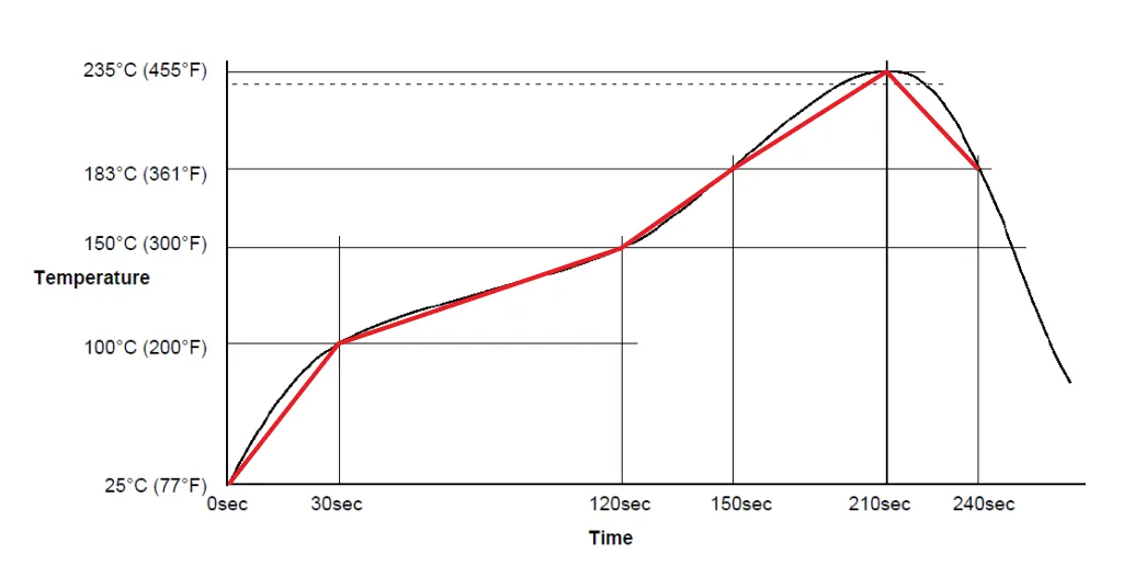
Common pitfalls include over-thick tin leading to uneven IMC, or contaminated plating baths fostering whiskers. Rework demands low-heat tools to avoid further IMC growth. These steps ensure robust immersion tin reflow soldering outcomes.
Conclusion
Reflow soldering profoundly shapes IMC formation in immersion tin, with Cu6Sn5 and Cu3Sn dictating joint strength and solderability after reflow. Balancing tin preservation against necessary bonding requires precise control of thermal profiles and atmospheres. Thermal cycling underscores the need for thin, uniform IMCs to withstand fatigue. Electric engineers benefit from standards-guided practices, troubleshooting rooted in microscopy and testing. Prioritizing these ensures reliable assemblies, minimizing field failures from intermetallic compound excesses.
FAQs
Q1: What happens to IMC formation during immersion tin reflow soldering?
A1: Immersion tin reflow soldering melts the tin layer, enabling copper diffusion to form Cu6Sn5 scallops first, followed by Cu3Sn at the copper interface. The first cycle consumes most tin, thickening IMCs and altering surface properties. Engineers control this via reflow time above liquidus to maintain balance. Excessive growth impairs wetting in subsequent steps.
Q2: How does solderability after reflow change with immersion tin?
A2: Solderability after reflow degrades as tin depletes, exposing Cu6Sn5 and Cu3Sn IMCs with inferior wetting. Multiple cycles accelerate this, causing de-wetting on pads. Flux selection and nitrogen reflow mitigate issues effectively. Testing per standards verifies performance post-assembly.
Q3: Why is thermal cycling critical for intermetallic compound growth in immersion tin?
A3: Thermal cycling promotes Cu3Sn thickening and Cu6Sn5 spalling via diffusion, weakening joints over cycles. Initial IMC from reflow soldering sets vulnerability. Optimized profiles and finishes enhance endurance. Shear tests quantify reliability impacts accurately.
Q4: What role do Cu3Sn and Cu6Sn5 play in immersion tin reliability?
A4: Cu6Sn5 provides initial bonding in immersion tin reflow soldering, while Cu3Sn grows brittle layers reducing ductility under thermal cycling. Balanced thickness ensures strength without cracking. Monitoring via cross-sections guides process tweaks. Standards like IPC-4554 aid compliance.
References
IPC-4554 — Specification for Immersion Tin. IPC, 2008
J-STD-020E — Moisture/Reflow Sensitivity Classification for Nonhermetic Surface Mount Devices. JEDEC, 2014
IPC J-STD-001G — Requirements for Soldered Electrical and Electronic Assemblies. IPC, 2017





