 ALLPCB


Introduction
Wearable fitness devices rely on compact printed circuit boards (PCBs) to integrate sensors, processors, and wireless modules into form factors that prioritize user comfort and battery life. These devices process high-speed digital signals from accelerometers, heart rate monitors, and gyroscopes while transmitting data via Bluetooth Low Energy protocols. Signal integrity challenges arise from the dense layouts, thin substrates, and proximity to the human body, which can introduce noise and interference. Engineers must address these issues early in the design phase to ensure reliable performance, data accuracy, and regulatory compliance. This article explores the principles behind signal integrity in wearable PCBs, common causes of degradation, and proven strategies for mitigation. By focusing on impedance control and electromagnetic interference reduction, designers can achieve robust signal transmission in fitness trackers.
The relevance intensifies with the push for smaller, lighter devices using rigid-flex or flexible substrates. These materials introduce variability in dielectric constants, complicating signal propagation. Engineers evaluate signal integrity through metrics such as eye diagram height, jitter, and return loss. Fitness trackers demand low-latency data processing, making every nanosecond of delay or distortion consequential. Ultimately, robust signal integrity supports the device's core functions, from real-time activity tracking to seamless app synchronization.
Understanding Signal Integrity in Wearable Fitness Device PCBs
Signal integrity refers to the preservation of electrical signal quality across a PCB, encompassing aspects like waveform shape, timing, and noise levels. In wearable fitness devices, signal integrity PCB wearable device performance directly impacts user experience, as degraded signals lead to erroneous heart rate readings or dropped Bluetooth connections. High data rates from sensor fusion and wireless communication exacerbate issues like reflections and crosstalk in confined spaces. Why does this matter? Poor signal integrity results in bit errors, increased power consumption from retransmissions, and shortened battery life, all critical in battery-constrained wearables. Adhering to established design principles ensures signals maintain their intended characteristics from source to receiver.
The relevance intensifies with the push for smaller, lighter devices using rigid-flex or flexible substrates. These materials introduce variability in dielectric constants, complicating signal propagation. Engineers evaluate signal integrity through metrics such as eye diagram height, jitter, and return loss. Fitness trackers demand low-latency data processing, making every nanosecond of delay or distortion consequential. Ultimately, robust signal integrity supports the device's core functions, from real-time activity tracking to seamless app synchronization.
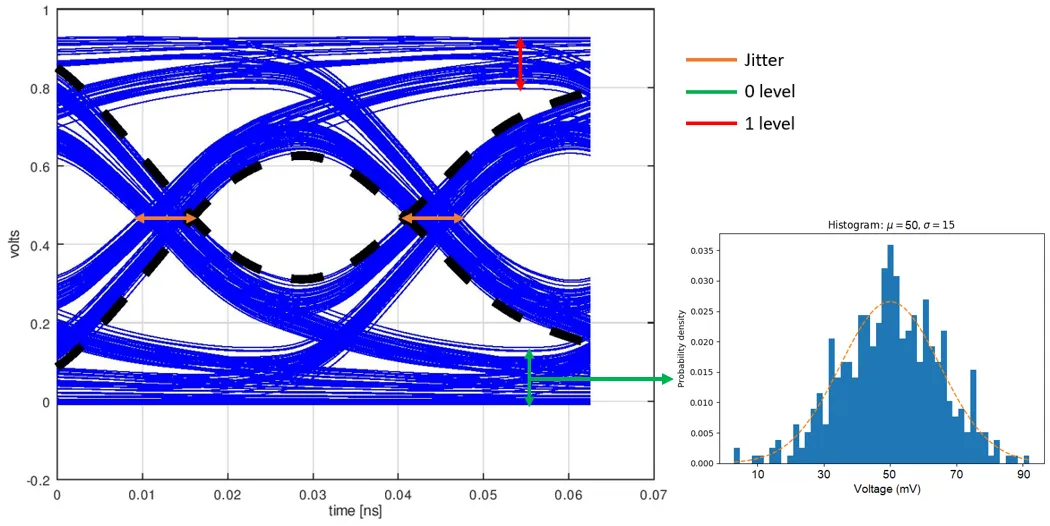
Key Causes of Signal Integrity Degradation
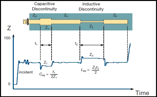
Several mechanisms contribute to signal degradation in wearable PCBs. Impedance discontinuities, such as those at vias, bends, or transitions between trace geometries, cause reflections that distort waveforms. In fitness trackers, where traces are narrow to fit tiny footprints, these mismatches amplify ringing and overshoot. Crosstalk occurs when aggressive coupling between adjacent traces induces noise on victim signals, particularly in multilayer stacks with shared reference planes. High-frequency components like crystal oscillators and RF antennas further couple energy into unintended paths.
Electromagnetic interference (EMI) poses a unique challenge in wearables due to the body's conductive properties acting as an antenna. External sources, including nearby smartphones or Wi-Fi, couple into unshielded traces, degrading signal-to-noise ratios. Ground bounce from simultaneous switching outputs creates voltage fluctuations on power planes, propagating as noise. Material inconsistencies, like variations in glass transition temperature, alter propagation delays over temperature cycles experienced during wear. Identifying these causes requires time-domain reflectometry and near-field scanning during prototyping.
Power delivery networks in compact devices introduce simultaneous switching noise, coupling into signal lines via shared vias. Flexing of rigid-flex boards shifts trace positions, varying coupling capacitance dynamically. Engineers must model these effects using field solvers to predict behavior before fabrication.
Technical Principles Governing Signal Integrity
Transmission line theory underpins signal integrity analysis, treating PCB traces as distributed RLC networks at high frequencies. Characteristic impedance, defined by trace width, thickness, and dielectric properties, determines reflection coefficients at discontinuities. For single-ended signals common in sensor interfaces, 50 ohms is typical, while differential pairs for LVDS or USB use 100 ohms. IPC-2141A provides guidelines for calculating and verifying controlled impedance, emphasizing stackup symmetry and reference plane proximity.
Propagation delay and attenuation depend on dielectric constant (Dk) and loss tangent (Df), with low-Dk materials preferred for wearables to minimize latency. Skin effect confines current to trace surfaces at gigahertz frequencies, increasing effective resistance and losses. Dispersion causes different frequency components to travel at varying speeds, closing eye openings. Return paths through ground planes must remain continuous to avoid inductive loops that radiate EMI.
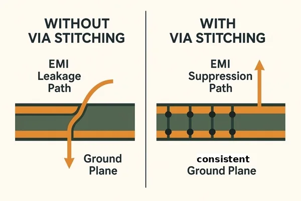
In mixed-signal designs, analog sensor traces require separation from digital clocks to prevent noise injection. Ground plane splits demand stitching vias to maintain low-impedance returns. Thermal expansion mismatches between copper and substrate create micro-cracks, altering impedance over time.
Best Practices for Impedance Matching in Fitness Tracker PCBs
Impedance matching PCB fitness tracker designs begins with stackup optimization, placing high-speed signals between ground or power planes for stripline configurations. Microstrip routing suits top-layer traces but exposes them to air-dielectric interfaces, requiring precise width calculations. Engineers specify tolerances like ±10% impedance to account for manufacturing variations in etch rates and plating. Field solver tools simulate stackups, adjusting core and prepreg thicknesses iteratively.
Routing strategies minimize vias by using blind or buried types, reducing stub lengths that act as resonators. Differential pairs maintain constant spacing and length matching within 5 mils to preserve common-mode rejection. Avoid right-angle bends; use 45-degree miters or curves to reduce reflections. For fitness trackers, group related signals—sensor data on inner layers, RF on outer—to control coupling.
Material selection favors low-loss laminates with stable Dk over frequency and temperature. Vias require back-drilling or filled designs to eliminate stubs in high-speed paths. Test coupons on panels verify impedance post-fabrication using TDR measurements.
Strategies for Reducing EMI in Wearable PCBs
Reducing EMI in wearable PCBs involves shielding, partitioning, and filtering at the board level. Solid ground planes under RF sections absorb stray fields, with via fences providing return current paths. Stitching vias along trace edges at lambda/20 spacing suppress slotline modes. Separate analog and digital grounds, connecting at a single point near the power entry to avoid loops.
Guard traces or moats isolate sensitive nodes, grounded at multiple points. Ferrite beads on power lines attenuate high-frequency noise without affecting DC. Component placement positions noisy elements like DC-DC converters away from antennas. Enclosures with conductive gaskets enhance overall shielding effectiveness.
Compliance testing per IEC standards validates emissions, but proactive design minimizes redesigns. Power plane capacitance, from thin dielectrics, decouples supplies effectively.
Troubleshooting Signal Integrity Issues
When issues arise, start with eye diagram analysis to quantify jitter and amplitude margins. TDR identifies impedance bumps correlating to layout features. Near-field probes localize EMI sources, guiding fixes like rerouting. Simulation-pre versus post-layout compares predictions to measurements, highlighting parasitics.
Common pitfalls include inadequate decoupling, fixed by adding 0402 capacitors near IC pins. Flex-induced shifts demand strain-relief routing. Iterative prototyping with flying probe tests refines designs. IPC-2221B outlines layout principles that prevent many issues upfront.
Conclusion
Solving signal integrity issues in wearable fitness device PCBs demands a holistic approach integrating controlled impedance, EMI mitigation, and rigorous verification. Key practices like optimized stackups, precise routing, and ground plane strategies ensure reliable high-speed performance. Engineers benefit from referencing IPC-2141A for impedance design and IPC-2221B for general guidelines. These methods not only enhance data accuracy in fitness trackers but also extend device reliability. Prioritizing signal integrity from concept to production yields devices that perform consistently in real-world conditions.
FAQs
Q1: What are the main causes of poor signal integrity PCB wearable device performance?
A1: Signal integrity degradation stems from impedance mismatches at vias and bends, crosstalk between dense traces, and EMI from body proximity or external sources. Reflections distort waveforms, while ground bounce adds jitter. In fitness trackers, high data rates amplify these effects. Addressing them requires controlled stackups and reference planes per IPC guidelines. Proactive simulation prevents field failures.
Q2: How does impedance matching PCB fitness tracker designs improve reliability?
A2: Impedance matching ensures minimal reflections, preserving signal shape and timing for accurate sensor data. Use stripline configurations with symmetric dielectrics for 50-ohm single-ended or 100-ohm differential traces. Manufacturing tolerances demand test coupons for verification. This reduces bit errors in Bluetooth links and processor interfaces. Consistent impedance supports low-power operation critical for wearables.
Q3: What techniques are effective for reducing EMI in wearable PCBs?
A3: Effective EMI reduction involves ground stitching vias, guard traces, and ferrite filtering on supplies. Partition analog and digital sections with moats connected at one point. Solid reference planes under RF traces absorb fields. Component placement away from antennas minimizes coupling. These practices maintain low emissions during body-worn use.
Q4: Why reference IPC standards in signal integrity PCB wearable device design?
A4: IPC standards like IPC-2141A provide proven methods for controlled impedance and high-speed layout. They ensure consistency across designs, aiding manufacturability and performance prediction. Guidelines cover trace spacing, via usage, and material effects. Following them reduces risks in compact fitness devices. Compliance builds confidence in reliability.
References
IPC-2141A — Design Guide for High-Speed Controlled Impedance Circuit Boards. IPC, 2004
IPC-2221B — Generic Standard on Printed Board Design. IPC, 2012
IPC-6012E — Qualification and Performance Specification for Rigid Printed Boards. IPC, 2017





