ALLPCB


Introduction
In PCB assembly, applying solder paste accurately sets the foundation for reliable solder joints and overall process yield. Traditional stencil printing has long dominated high-volume surface mount technology lines due to its speed and consistency. However, solder paste jet printing emerges as a non-contact alternative that promises greater flexibility for complex designs. This method ejects precise droplets of solder paste directly onto pads, eliminating many stencil-related challenges. Electric engineers evaluating assembly options must weigh jet printing's potential against established practices to optimize production workflows. As boards grow denser with finer pitches and varied deposit volumes, jet printing gains traction in prototyping and high-mix environments.
What Is Solder Paste Jet Printing and Why Does It Matter?
Solder paste jet printing involves using specialized equipment to propel micro-droplets of solder paste onto PCB pads without physical contact. Unlike stencil methods, it relies on software-controlled nozzles that adjust deposit volume and shape in real-time. This technology suits applications demanding variable paste heights, such as stepped stencils or multi-level components. Engineers value it for rapid prototyping, where frequent design changes occur, reducing setup times significantly. In high-mix low-volume production, jet printing minimizes material waste by applying only the required paste amount. Its relevance grows with shrinking component sizes, enabling precise high-speed solder paste application on fine-pitch arrays.
The shift matters because stencil printing struggles with board warpage, flexible substrates, and odd-shaped pads. Jet printing overcomes these by maintaining consistent deposits regardless of surface irregularities. Production teams report fewer defects from paste bridging or insufficient volume, improving first-pass yields. For electric engineers troubleshooting assembly lines, this method offers diagnostic insights through programmable parameters. Ultimately, it aligns with demands for agile manufacturing in evolving electronics sectors.
Technical Principles of Solder Paste Jet Printing
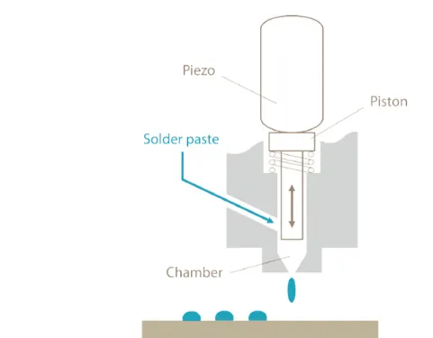
At its core, solder paste jet printing uses piezoelectric or piston-driven mechanisms to generate pressure waves that eject solder paste from nozzles. The paste, typically Type 5 or 6 with finer particles for better flow, must exhibit thixotropic properties to form stable droplets post-ejection. Droplet size ranges from tens to hundreds of microns, controlled by nozzle diameter, pressure, and viscosity. The system scans the PCB, aligning jets with fiducials for sub-micron accuracy. Rheology plays a critical role, as high metal content pastes demand optimized formulations to prevent clogging during continuous operation.
In operation, the jet head moves over the board while firing droplets at rates supporting high-speed solder paste application. Software integrates with CAD data to vary volume per pad, enabling 3D deposit profiles. This non-contact nature avoids stencil-to-board separation issues like paste smearing. Engineers must calibrate jet velocity to match paste tackiness, ensuring adhesion without satellite droplets. Thermal management of the paste cartridge maintains consistency, as temperature fluctuations alter viscosity. These principles enable jet printing to handle diverse substrates, from rigid FR-4 to flex circuits.
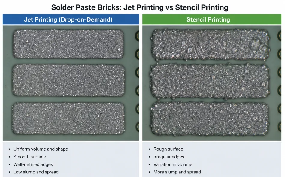
Jet Printing vs Stencil Printing: A Direct Comparison
Stencil printing forces paste through apertures using squeegees, ideal for uniform high-volume runs but prone to wear and cleaning cycles. Jet printing dispenses droplets individually, offering instant programmability without hardware changes. In jet printing vs stencil printing debates, the former excels in flexibility for prototype iterations, while the latter dominates mass production throughput. Stencil methods require precise alignment and flatness to avoid defects like bridging, whereas jetting accommodates warped boards up to certain tolerances. Engineers note stencil cleaning consumes time and solvent, contrasting jet printing's cartridge-based paste handling.
Volume control highlights key differences: stencils deliver fixed amounts per aperture, necessitating multi-level designs for variations, while jet printing adjusts dynamically. For fine-pitch components under 0.3mm, jetting provides superior precision without aperture collapse risks. However, stencil's proven scalability suits automotive volumes, per IPC J-STD-001 soldering requirements. Troubleshooting stencil defects often traces to paste release, resolvable in jetting via droplet tuning. Overall, hybrid approaches emerge where jet supplements stencil for outliers.
Related Reading: Stencil Printing vs. Jet Printing: Which Method is Best for Your PCB Assembly Needs?
Advantages of Jet Printing in PCB Assembly
One primary advantage of jet printing lies in eliminating stencil fabrication and maintenance costs, streamlining low-volume workflows. Engineers appreciate the ability to deposit variable volumes, from micro-dots to larger bridges, without hardware swaps. This supports high-mix production, reducing changeover times to minutes via software updates. Non-contact application prevents board damage, crucial for thin flex or warped panels. Paste waste drops as only targeted amounts apply, enhancing material efficiency.
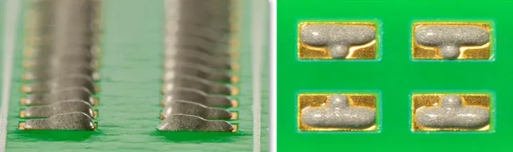
Precision shines in fine-pitch and heterogeneous assemblies, achieving consistent deposits for BGA or QFN parts. Real-time monitoring allows volume adjustments mid-print, minimizing defects traceable to IPC-A-610 acceptability criteria. High-speed solder paste application reaches rates suitable for mid-volume lines, with dot frequencies exceeding hundreds per second. Flexibility extends to adhesives or encapsulants on the same machine, consolidating equipment footprints. For troubleshooting, jet data logs aid root-cause analysis of joint voids or slumps.
Related Reading: The Ultimate Guide to Solder Paste Types for PCB Assembly
Disadvantages of Jet Printing and Limitations
Despite benefits, jet printing lags in throughput for ultra-high-volume lines, as individual droplet formation slows versus squeegee sweeps. Solder paste requirements narrow to low-viscosity Type 5/6 formulations, limiting alloy choices and increasing costs. Nozzle maintenance demands regular checks to avert clogs from particle settling, potentially halting production. Initial equipment investment exceeds basic stencil printers, challenging small-scale adopters. Engineers report sensitivity to environmental factors like humidity affecting paste stability.
Scalability issues arise in matching stencil's uniformity across large panels, requiring validation per J-STD-005 paste specifications. Paste cartridge life and refill frequency add operational overhead. For coarse-pitch high-alloy pastes, jetting underperforms due to rheology mismatches. Troubleshooting demands specialized training on jet parameters, unlike intuitive stencil tweaks. These factors position jet printing best as a complementary tool.
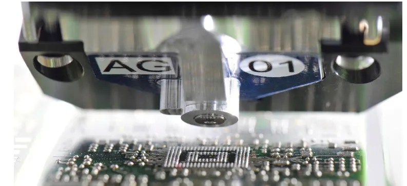
Solder Paste Jet Printing Machines and High-Speed Application
Solder paste jet printing machines integrate vision systems, motion control, and jet heads for automated deposition. Multi-nozzle arrays boost throughput, targeting high-speed solder paste application in dynamic lines. Cartridge-fed systems ensure consistent paste supply, with heaters maintaining optimal viscosity. Fiducial recognition compensates for board stretch or shift, vital for precision. Software interfaces with MES for traceability, logging deposit stats per pad.
In high-speed modes, machines achieve dot rates supporting mid-volume SMT, ideal for NPI transitions. Dual-mode operation switches between jetting paste and dispensing glue seamlessly. Engineers optimize paths to minimize travel, enhancing cycle times. Integration with pick-and-place lines requires synchronized data exchange. Robustness against vibration ensures reliability in factory settings.
Best Practices and Troubleshooting for Solder Paste Jet Printing
Select paste matching machine specs, verifying rheology via slump and viscosity tests per J-STD-005. Calibrate nozzles daily, monitoring droplet weight for repeatability. Maintain 20-25°C cartridge temperature to stabilize flow. Use vision inspection post-print to verify brick height and alignment against IPC-A-610 Class 2/3 criteria. For warpage, enable height mapping to adjust z-axis dynamically.
Troubleshooting starts with void analysis: increase droplet size or velocity if insufficient volume. Bridging signals over-deposition; reduce frequency or spacing. Clogs trace to dry paste; purge and clean nozzles promptly. Log reflow profiles to correlate paste performance with joint quality per IPC J-STD-001. Validate process with SPI, targeting 75-125% volume efficiency. Train operators on parameter interlinks for proactive tweaks.
Conclusion
Solder paste jet printing revolutionizes PCB assembly by offering stencil-free flexibility and precision for challenging designs. While excelling in prototypes and high-mix scenarios, it complements rather than replaces stencil for mass production. Electric engineers benefit from its troubleshooting diagnostics and defect reduction potential. Balancing advantages like variable deposits against throughput limits guides optimal adoption. As components miniaturize, jet printing's role expands, enhancing overall yield and agility. Future integrations promise even higher speeds, solidifying its place in modern SMT.
FAQs
Q1: What are the main advantages of jet printing over stencil printing for solder paste application?
A1: Jet printing eliminates stencil costs and wear, enables real-time volume adjustments, and handles warped or flexible boards without contact. It reduces waste and suits fine-pitch components, improving yields in high-mix production. Per practical experience, changeovers drop to software edits, minimizing downtime. This makes it ideal for prototyping where stencil changes delay workflows.
Q2: What disadvantages should engineers consider with solder paste jet printing machines?
A2: Slower throughput limits high-volume use, and finer Type 5/6 pastes raise costs with specific rheology needs. Nozzle clogs require frequent maintenance, and upfront investment exceeds stencil setups. Troubleshooting demands parameter expertise to avoid defects like satellites. Still, mid-volume lines gain from its precision.
Q3: How does high-speed solder paste application work in jet printing?
A3: Multi-nozzle heads fire droplets at high frequencies while scanning boards, supported by fast motion control. Vision aligns with fiducials for accuracy, achieving rates for dynamic production. Optimize paste viscosity and pathing to maximize speed without quality loss. It excels where stencil struggles with complexity.
Q4: Is solder paste jet printing suitable for all PCB assembly types?
A4: Best for prototypes, flex circuits, and fine-pitch high-mix; less for uniform high-volume rigid boards. Evaluate per design: variable deposits favor jetting. Validate joints against IPC standards for reliability. Hybrid use often optimizes overall lines.
References
IPC J-STD-001 — Requirements for Soldered Electrical and Electronic Assemblies. IPC.
IPC-A-610 — Acceptability of Electronic Assemblies. IPC.
J-STD-005 — Requirements for Soldering Pastes. IPC.