ALLPCB


Introduction
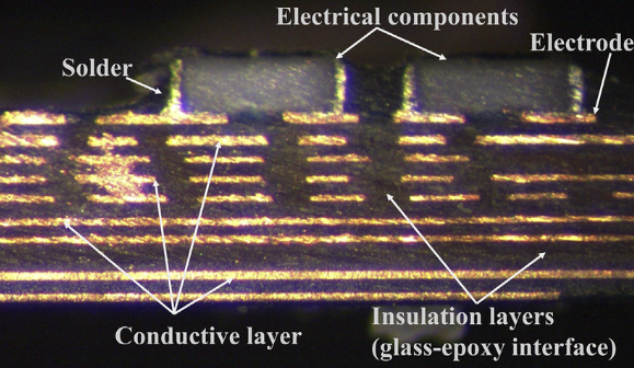
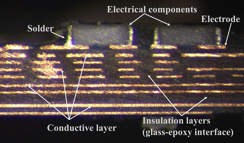
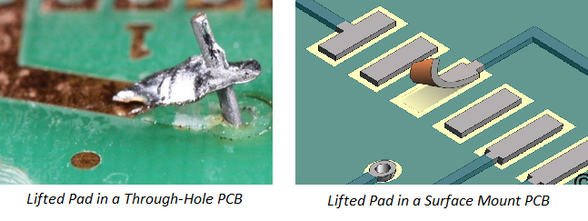
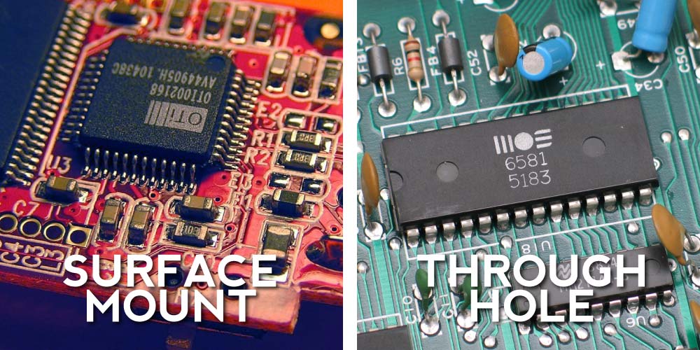
Printed circuit boards (PCBs) integrate surface-mount devices (SMD) and through-hole (TH) components to meet diverse performance needs in electronic assemblies. Repairing these boards requires selecting techniques that match the component type to avoid damage like delamination or lifted pads. SMD rework techniques focus on precise heat application for densely packed parts, while through-hole component removal demands methods that clear solder from vias without stressing the board. Understanding these differences ensures reliability in high-volume production or field service environments. This article compares SMD and through-hole repair processes, highlighting best practices for electric engineers facing rework challenges. By aligning repair methods with PCB technology, engineers can minimize downtime and maintain assembly integrity.
Understanding SMD and Through-Hole Technologies
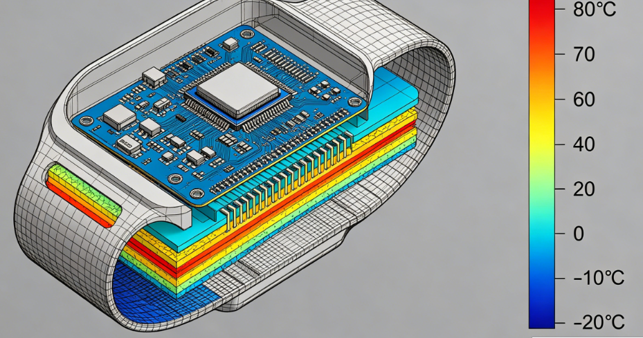
Surface-mount devices attach directly to the PCB surface using solder paste reflowed in ovens, enabling compact designs with high component density. Through-hole components feature leads passing through board holes, soldered on the opposite side for mechanical strength in applications like power electronics. SMD assemblies dominate modern consumer electronics due to miniaturization, but TH persists in rugged environments requiring vibration resistance. Repair complexity arises from these attachment differences: SMD joints are fillet-based and heat-sensitive, while TH involves barrel solder that can wick into vias. Engineers must assess board stack-up and layer count before repair to predict thermal responses. Proper technique selection prevents issues like tombstoning in SMD or hole enlargement in TH.
Fundamentals of SMD Rework Techniques
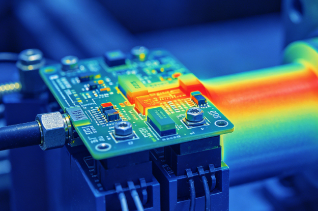
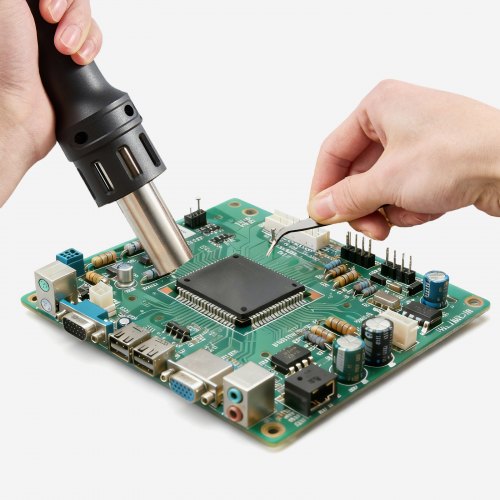
SMD rework techniques prioritize non-contact heating to reflow solder without mechanical force, preserving nearby components. Hot air rework for SMD repair uses a focused stream of heated nitrogen or air to melt joints uniformly, typically starting with preheating the board to 100-150°C to reduce thermal shock. Apply low-residue flux to activate solder and prevent oxidation, then position a nozzle over the component for 30-60 seconds at 250-350°C, depending on alloy. Lift the part with vacuum tweezers once molten, clean pads with braid, and align the replacement before final reflow. IPC-7711/7721 outlines procedures for component removal and replacement, emphasizing temperature profiling to avoid exceeding 260°C peak for lead-free solder. This method suits QFN, BGA, and passives but requires airflow control to prevent warpage on multilayer boards.
Infrared (IR) or conduction heating complements hot air for larger SMDs, providing stable profiles monitored by thermocouples. Convection ovens offer batch rework for prototypes, ensuring even heat distribution across the assembly. Post-rework inspection verifies fillet formation and void-free joints per acceptability criteria. Engineers often profile the process using data loggers to replicate reflow conditions, minimizing risks like pad cratering.
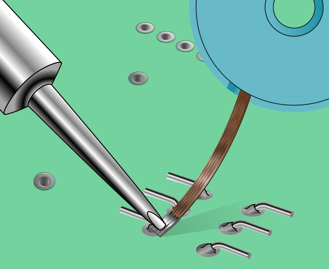
Fundamentals of Through-Hole Component Removal and Repair
Through-hole component removal starts with desoldering techniques that extract molten solder from holes while gripping the lead. A powered desoldering tool with vacuum suction heats pins sequentially, flooding joints with flux to lower viscosity and improve flow. Maintain iron tip at 350-400°C for 3-5 seconds per pin, sucking solder as it liquefies to avoid bridging adjacent holes. For multi-pin devices like connectors, twin-tip irons heat two sides simultaneously, reducing cycle time. IPC-7711/7721 details steps for TH removal, including hole cleaning with wire brushes or pumps to restore drill size integrity. After extraction, inspect vias for plating damage and replate if barrel integrity is compromised.
Solder wick or pumps handle cleanup for stubborn residue, wicking alloy under flux activation. Replacement involves wave soldering simulation with hand irons, forming smooth heels and toes on fillets. J-STD-001 specifies criteria for TH solder joints, such as 100% hole fill and minimum barrel coverage. This process suits axial leads, DIPs, and headers but demands patience to prevent lead bending or board flexure.
Comparing SMD and Through-Hole Repair Processes
Comparing SMD and through-hole repair processes reveals trade-offs in speed, precision, and risk. SMD rework techniques like hot air allow parallel heating for arrays, completing in seconds versus minutes for TH desoldering per pin. TH removal risks mechanical stress on vias, potentially cracking inner layers, while SMD heat can cause coefficient of thermal expansion mismatch leading to warpage. Tooling differs: SMD uses nozzles and profiles, TH relies on tips and suction. Thermal demands vary, with SMD peaking lower but requiring ramps, and TH tolerating higher locals but longer dwells. IPC-A-610 provides visual criteria for both, ensuring post-repair joints meet class 2 or 3 requirements.
Aspect - SMD Repair: Non-contact (hot air, IR); Through-Hole Repair: Contact (iron, desolder gun)
Time per Component - SMD Repair: 30-120 seconds; Through-Hole Repair: 10-30 seconds per pin
Primary Risks - SMD Repair: Warpage, component shift; Through-Hole Repair: Via damage, bridging
Cleanup Method - SMD Repair: Braid, alcohol wipe; Through-Hole Repair: Wick, pump, brushing
Standards Reference - SMD Repair: IPC-7711/7721 for reflow profiles; Through-Hole Repair: J-STD-001 for fillet specs
SMD suits high-density boards but demands cleanrooms for flux residue control, whereas TH excels in low-volume fixes with forgiving tolerances.
Best Practices for Effective PCB Repair
Preheat all boards to 80-120°C for 5-10 minutes to equalize temperatures and reduce gradients. Use no-clean flux sparingly to avoid ionic contamination, activating only at joint interfaces. Profile every rework station with thermocouples, targeting 1-2°C/s ramps and 60-second above-liquidus times. For SMD, employ bottom-side heaters to stabilize multilayer stacks; for TH, clip leads short before desoldering to minimize wicking. Clean and tin pads immediately post-removal to prevent oxidation, then bake replacements if moisture-sensitive. Document profiles and inspect under 10x magnification for voids or cold joints.
Mask sensitive areas with high-temperature tape during hot air rework for SMD repair. Verify ESD controls and humidity below 50% to protect components. Train operators on sequential heating for TH multi-leads, rotating pins to uniform melt.
Common Challenges in PCB Repair and Troubleshooting Tips
Warpage plagues SMD rework on thin flex boards; mitigate with fixturing and dual-sided heating. TH desoldering often leaves solder balls; flood with flux and vacuum repeatedly. Component tombstoning in SMD arises from uneven heating; adjust airflow and preheat higher. Bridging in dense SMD arrays requires precise nozzle sizing and post-clean with isopropyl. Via plating lift in TH signals overheat; limit dwell and use low-melt alloys if possible. Troubleshooting involves root-cause analysis: log temperatures, flux type, and board specs for repeatability.
Lift failures trace to poor flux activation; switch to rosin mildly activated formulas. Always validate with electrical tests post-repair.
Conclusion
Choosing between SMD rework techniques and through-hole component removal hinges on board design, component pitch, and production volume. Hot air methods excel for SMD density, while desoldering tools dominate TH robustness. Adhering to standards like IPC-7711/7721 ensures consistent quality across repairs. Engineers benefit from profiling, preheating, and meticulous cleanup to extend PCB life. Mastering these processes optimizes reliability in evolving electronics landscapes.
FAQs
Q1: What are the key SMD rework techniques for electric engineers?
A1: SMD rework techniques include hot air rework for SMD repair, infrared heating, and conduction methods, each suited to component size and density. Preheat the board, apply flux, and use vacuum lift for removal per IPC-7711/7721 guidelines. Profile temperatures to match reflow, clean pads, and reinspect joints for voids to minimize thermal stress on high-density assemblies.
Q2: How do you perform through-hole component removal without damaging the PCB?
A2: Through-hole component removal uses desoldering irons with vacuum, heating pins sequentially after flux application. Maintain 350-400°C for 3-5 seconds per side, suck solder, and brush holes clean. Avoid overheating to preserve plating per J-STD-001. For multi-pins, use dual tips and rotate for even melt, then inspect for barrel integrity afterward.
Q3: What factors should be considered when comparing SMD and through-hole repair processes?
A3: Consider heat application type, cycle time, and risks. SMD favors non-contact hot air for speed on dense boards; TH relies on contact desoldering for via clearance. SMD risks warpage and component shift; TH risks inner-layer damage and bridging. Use standards like IPC-A-610 for acceptability and preheat universally for best results.
Q4: Can hot air be used for through-hole desoldering?
A4: Hot air can be applied to through-hole work but is less efficient than dedicated desoldering tools, risking uneven melt and adjacent component damage. Use wider nozzles at higher flows for pins, combined with wick cleanup. Prefer vacuum desoldering guns for precision per IPC-7711/7721, and limit use to low pin counts to reduce board stress.
References
IPC-7711/7721 - Rework, Modification and Repair of Electronic Assemblies. IPC
J-STD-001 - Requirements for Soldered Electrical and Electronic Assemblies. IPC
IPC-A-610 - Acceptability of Electronic Assemblies. IPC