 ALLPCB


Abstract
Compared with silicon, SiC offers a wider bandgap, higher thermal conductivity, higher breakdown field, and higher electron saturation velocity, making it suitable for high-temperature, high-voltage, high-current, high-frequency power devices. Traditional wire bonding is one of the most common interconnect methods for power devices. However, wire bonding introduces parasitic inductance and thermal limitations that constrain SiC device performance. This article first reviews low-parasitic-inductance and efficient-cooling interconnect techniques developed for silicon power devices, then surveys interconnect techniques for SiC power devices, and finally summarizes the remaining challenges for SiC device interconnects.
1. Introduction
Compared with silicon devices, SiC devices provide higher temperature tolerance, larger breakdown voltage, and faster switching capability, enabling operation at higher switching frequencies. These advantages, however, also create challenges for interconnects and packaging of SiC power devices.
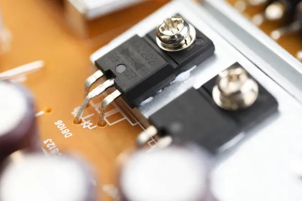
Aluminum wire bonding remains the most common interconnect form for power devices. The device bottom is attached via solder and Direct-Bonded Copper (DBC) and the top is connected by wire bonds. The parasitic inductance introduced by this interconnect can exceed 10 nH. Large di/dt during switching can cause voltage overshoot, increase switching losses, produce electromagnetic interference, and distort switching waveforms. From a thermal perspective, heat generated by the power device is primarily removed through the bottom, which limits thermal performance. As switching frequency increases, switching power loss increases, motivating development of low-parasitic-inductance and high-efficiency cooling interconnect solutions.
2. SiC Device Characteristics and Advantages
Compared with silicon, the bandgap of 4H-SiC is about three times larger while its intrinsic carrier concentration is much lower. The wide bandgap and low intrinsic carrier concentration allow SiC devices to operate at higher temperatures. The breakdown field of 4H-SiC is an order of magnitude higher than silicon, enabling higher voltage capability. Table 1 lists the basic properties of common semiconductor materials.
A variety of SiC devices have been developed, including MOSFETs, Schottky diodes, JFETs, and insulated-gate bipolar transistors (IGBTs). Among these, SiC MOSFETs have attracted significant attention for their favorable performance.
SiC MOSFETs switch faster and have relatively low switching loss, making them suitable for high-frequency environments. By contrast, IGBTs have bipolar characteristics that result in slower switching and higher switching loss. Compared with silicon IGBTs, SiC MOSFETs have higher drift-region doping and lower conduction loss. SiC MOSFETs also exhibit lower output capacitance and gate charge, enabling faster dv/dt and di/dt transitions. Higher switching speed allows higher switching frequency, increasing power density and efficiency. In addition, the switching loss of silicon IGBTs increases significantly at elevated junction temperatures, whereas SiC MOSFET switching loss changes less with temperature.
3. Silicon-based Power Device Interconnect Forms
Interconnects developed for silicon power devices provide a foundation for SiC device interconnects. Mature silicon interconnect approaches include planar interconnects, copper-clip interconnects, and chip-embedded interconnects, with some stacked structures used to increase power density and reduce parasitics. These approaches often involve more complex processes and higher cost.
3.1 Planar Interconnect Packaging
There are many planar interconnect packaging variants. Notable examples include Siemens' planar interconnect packaging and multilayer planar interconnects. Siemens' SiPLIT technology uses thick copper and insulating layers above the power die, reducing parasitic inductance and increasing thermal contact area. Electrical and thermal characterization showed parasitic inductance reduced by about 50% and thermal resistance reduced by about 20%.
3.2 Copper-clip Interconnect
Copper-clip interconnects are another typical planar approach. Flat copper clips have been used to replace traditional aluminum wire bonds. Due to copper's high electrical and thermal conductivity, copper clips reduce parasitic inductance and provide an additional thermal path through the chip top surface. In single-sided cooling tests, junction-to-case thermal resistance for a single die decreased by 23% compared with aluminum wire bonding; for two parallel dies the thermal resistance decreased by about 18%. In dual-sided cooling experiments, adding a top heatsink and fan to the copper clip improved average cooling performance by about 18%.
3.3 Chip-embedded Interconnect
An embedded power device structure where multiple power dies, such as IGBTs, MOSFETs, and diodes, are embedded into a ceramic substrate frame and covered by a dielectric layer. Multilayer metallization is deposited on the surface to contact die pads. The process uses sputtered Ti and Cu followed by electroplated thicker copper layers. Compared with traditional wire bonding, this embedded interconnect form reduces parasitic inductance by 75% and improves thermal efficiency by 44%.
4. SiC Power Device Interconnect Techniques
Multiple interconnect forms for SiC power devices have emerged, including planar interconnects, 3-D interconnects, and hybrid packaging. The trend for commercialization is toward economical, high-reliability, high-density interconnect methods.
4.1 Planar Interconnect Techniques
4.1.1 Miniaturized Dual-sided Cooling
D.R.M. Woo et al. developed a miniaturized dual-sided cooling interconnect scheme for high-temperature SiC power inverter dies, capable of over 220 °C operation. Bismuth-silver solder paste was used to realize flip-chip bonding for source and gate connections. The solidus is about 260 °C and the liquidus about 360 °C, offering higher thermal stability than conventional lead-free solders. To improve wetting of the solder paste, electroless nickel immersion gold was applied to Al pads. Drain interconnects used silver sinter materials to attach copper clips. Thermal modeling and characterization showed about a twofold improvement in heat dissipation compared with conventional single-sided-cooled devices.
4.1.2 Stacked Interconnect Packaging
In 2018, GE proposed a kilowatt-scale SiC interconnect scheme called PowerOverlay kiloWatt (POLkW). Typical device structure uses copper vias on polyimide film as interconnects between dies and wiring layers. Adhesives attach the dies to the polyimide film. Laser-drilled vias are plated to fill the vias. A DBC substrate with Ni/Au surface treatment is soldered to the die backside (Ag surface treatment). Underfill is used for electrical isolation and mechanical reinforcement. Compared with wire-bonded interconnects, polyimide-based copper interconnects greatly improve copper utilization, reduce parasitic inductance, and help reduce switching loss and voltage overshoot.
4.1.3 LTCC-based Dual-sided Cooling
H. Zhang et al. proposed a bondless SiC power device interconnect capable of dual-sided cooling using an LTCC substrate as dielectric and die carrier. Power dies are connected to the top and bottom of a DBC substrate using nano-silver paste. Silver and copper are plated on the DBC top and bottom for connections; Cr/Ni/Ag layers are deposited on diode anodes and MOSFET source and gate. High-temperature dielectric fills gaps between the LTCC substrate and the dies to prevent breakdown during operation. Simulation results indicate that, under the same operating conditions, the LTCC-based dual-sided cooling module has lower thermal resistance than embedded power modules and PBGA modules.
4.2 3-D Interconnect Techniques
4.2.1 Flip-chip Interconnect
S. Seal and H. A. Mantooth developed a chip-scale, wire-free interconnect process for SiC Schottky diodes, reducing parasitics, cost, and loss while improving reliability. This method uses flip-chip solder ball arrays to connect the anode and copper to connect to the bottom cathode. Compared with wire-bonded interconnects, the wire-free interconnect reduced on-state resistance by 24%.
4.2.2 Copper-pin Interconnect
Fuji developed a copper-pin interconnect structure for SiC power modules. Traditional aluminum wire bonds, solder joints, and silicone interconnects were replaced by copper pins, silver sinter connections, and epoxy molding structures, respectively. To further reduce thermal resistance, thicker copper blocks were bonded to the silicon nitride ceramic substrate. Compared with alumina ceramic structures, the copper-pin structure reduced overall thermal resistance by 50%. Compared with traditional silicon wire-bonded interconnects, SiC devices using copper-pin structures showed loss reductions of 57% to 87%.
4.3 Hybrid Packaging Interconnects
4.3.1 DBC and PCB Hybrid Structure
A DBC and multilayer slotted PCB hybrid structure for SiC power modules has been proposed. A multilayer slotted PCB is attached on the DBC substrate, with SiC devices placed in recesses and attached to the DBC. Wire bonds are then used to connect top electrodes to top copper traces on the PCB.
4.3.2 DBC and FPC Hybrid Structure
A 1200 V, 120 A SiC bridge-arm power module using a DBC and flexible printed circuit (FPC) hybrid structure has been reported. It shows the hybrid structure and the switching loop associated with MOSFET Q1 and diode D2. Because opposing currents flow through the thin FPC board, magnetic coupling cancels strongly. By using a thin FPC and careful layout, the parasitic inductance of the power module can be reduced to 0.79 nH. Compared with commercial modules under the same decoupling capacitance and gate drive conditions, the hybrid module reduced voltage overshoot by about 50% and switching energy loss to approximately one third of the commercial module.
5. Challenges for SiC Power Device Interconnects
SiC power device interconnect technology has matured, but compared with traditional silicon-based interconnects, SiC requires stricter control of parasitic inductance and thermal dissipation. The unique characteristics of SiC devices, such as high-speed switching, present additional challenges in interconnect design and packaging.
Although SiC MOSFETs switch faster, are smaller, and have lower switching loss, they cannot always be directly substituted into existing silicon interconnects. Fast switching speed and thermal requirements of SiC MOSFETs pose major interconnect challenges. Development of new interconnect techniques also faces challenges in material selection and process integration. Quantitative measurement and characterization of new interconnect structures remain difficult. These issues must be addressed in SiC MOSFET interconnect design.
5.1 Fast Switching Speed
A comparative study evaluated silicon IGBTs and SiC MOSFETs of equal power rating from Infineon (third-generation IGBT IKW15N120H3) and Cree (SiC MOSFET C2M0080120D). Measured dv/dt and di/dt values indicate that SiC MOSFETs switch much faster than silicon IGBTs. Faster switching makes SiC device behavior more sensitive to parasitic elements such as inductance and capacitance.
5.2 Thermal Management
Switching frequencies for silicon IGBT-based converters are often limited to about 20 kHz, while SiC MOSFETs can operate at switching frequencies up to 100 kHz in converters. Due to smaller die size, power loss density at high frequency is higher, making thermal management more challenging for SiC devices. Traditional single-sided cooling is often insufficient. Novel dual- or multi-sided liquid cooling solutions show strong potential to maintain low die junction temperatures while addressing heat removal needs.
5.3 Material Selection
Although SiC devices can theoretically operate at temperatures up to 600 °C, current packaging materials limit practical junction temperatures to around 175 °C. Many packaging materials used for silicon power devices, such as die adhesives and sealants, cannot maintain long-term stability above 175 °C. In harsh environments with high ambient and operating temperatures, mismatched coefficients of thermal expansion (CTE) can cause excessive warpage, leading to die cracking and interface delamination. Therefore, interconnect materials for SiC power devices should be high-temperature stable, electrically insulating where needed, and CTE-matched.
5.4 Interconnect Processes
To achieve low parasitic inductance and efficient cooling, new wire-free interconnects and topologies are being developed, but they introduce process challenges and potential new failure modes.
Most commercially available SiC power devices are designed for Al wire bonding, with Al metallization on the front-side pads, which is incompatible with many wire-free interconnect processes. Additional metallization on the source and gate pads is required for wire-free interconnects. Re-metallization of Al pads at the wafer or die level typically uses sputtering or other physical vapor deposition to deposit one or more metallization layers on the original Al pad. For SiC MOSFETs, wafer- or die-level pad re-metallization is costly and risky. Small die sizes make die-level re-metallization difficult, and sputtering conditions must be tightly controlled to avoid poor adhesion that would cause interconnect failures. Thus, re-metallization of Al pads on SiC devices is a key challenge.
Bonding processes are also challenging. To improve thermal performance, soldering or sintering materials are often used, but their bonding conditions are hard to control. In multi-die bonding, poor process control can create many voids at the interface, degrading thermal performance.
6. Conclusion
High-power SiC modules are in demand for electric vehicles, photovoltaics, and battery energy storage systems. Traditional aluminum wire bonding introduces inherent parasitic inductance, thermal, and reliability issues; multi-die interconnects also raise cost concerns. The industry has developed many economical interconnect schemes that reduce parasitic inductance and improve cooling, including planar interconnects, 3-D interconnects, and embedded PCB interconnects. This article described SiC device performance and highlighted advantages of SiC material for high operating temperature and high switching frequency applications. It reviewed silicon-based interconnect schemes as a foundation and discussed SiC interconnect techniques that enable efficient cooling. Finally, it summarized the main challenges in materials and processes that must be addressed in the development of new SiC interconnect technologies.


