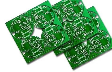
ALLPCB


Introduction
Rigid PCB trace routing forms the backbone of reliable circuit performance in electronic designs. Engineers focus on this process to balance electrical characteristics with production feasibility. Proper techniques ensure signals propagate without distortion while adhering to fabrication limits. In high-density boards, suboptimal routing leads to issues like crosstalk or yield losses. This article explores strategies for rigid PCB trace routing that enhance rigid PCB signal integrity and rigid PCB manufacturability. Readers gain actionable insights grounded in engineering principles.
What Is Rigid PCB Trace Routing and Why It Matters
Rigid PCB trace routing involves planning and laying out conductive paths on non-flexible printed circuit boards. These paths connect components and carry signals or power across layers. The process demands consideration of electrical, thermal, and mechanical factors. Poor routing compromises rigid PCB signal integrity through reflections, noise, or attenuation. It also affects rigid PCB manufacturability by increasing defects during etching or plating. Adhering to guidelines like those in IPC-2221 ensures designs meet performance and production standards.
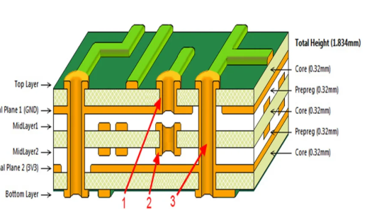
Engineers prioritize trace routing early in the design cycle to avoid costly revisions. Effective routing minimizes electromagnetic interference and supports higher frequencies. In multilayer rigid PCBs, vertical alignment between layers influences via reliability. Balancing density with clearances prevents short circuits and eases assembly. Ultimately, optimized rigid PCB trace routing drives product reliability and cost efficiency.
Fundamental Principles of Signal Integrity in Rigid PCB Trace Routing
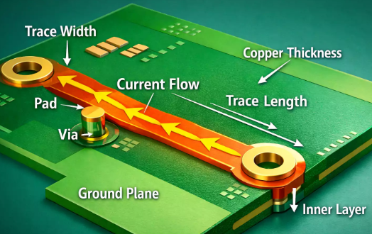
Signal integrity in rigid PCBs hinges on controlled impedance along traces. Impedance mismatches cause reflections that degrade waveforms. Engineers calculate characteristic impedance based on trace geometry, dielectric properties, and layer stackup. Maintaining consistent rigid PCB trace width prevents variations that disrupt signals. Ground planes adjacent to signal layers provide return paths and shield against crosstalk.
Crosstalk arises when parallel traces couple capacitively or inductively. Spacing traces at least three times their width reduces this effect. Length-matched routing preserves timing for differential pairs. Vias introduce discontinuities, so minimizing their use or employing back-drilling helps. These principles apply across frequencies, from DC to GHz ranges.

Thermal management intersects with signal integrity as current flow heats traces. Wider traces handle higher currents but alter impedance. IPC-2221 provides formulas relating trace width to allowable temperature rise. Engineers simulate these effects to predict performance under load.
Optimizing Rigid PCB Trace Width for Performance and Production
Rigid PCB trace width selection balances current capacity, impedance, and fabrication tolerances. Narrow traces suit high-density signals but risk overheating or etching defects. Wider traces improve power delivery yet consume board space. Standards guide minimum widths based on copper thickness and process capabilities. Consistent width along a net avoids impedance steps that reflect signals.
For signal lines, target 50-ohm single-ended or 100-ohm differential impedance common in many designs. Taper transitions gradually between widths to smooth impedance profiles. In power planes, segmented pours prevent voids during lamination. Engineers verify widths through stackup calculators tied to material properties.
Manufacturability favors widths above 0.1 mm for standard processes, though finer features demand advanced imaging. Aspect ratios in vias align with trace widths to ensure plating uniformity. IPC-A-600 criteria assess finished trace quality, rejecting undercuts or bridges.
Best Practices for Rigid PCB Trace Routing
Start routing with critical high-speed nets to secure optimal paths. Assign dedicated layers for signals, avoiding splits in ground planes. Use 45-degree bends over 90-degree corners to reduce reflections, though curved arcs offer even better results for GHz signals. Fanouts from components follow grid alignments for drill accuracy.
Group analog and digital traces separately to isolate noise domains. Perforate planes under sensitive traces to cut capacitive coupling. Length tuning compensates delays, matching pairs within picoseconds. Simulate pre-layout to identify hotspots.
For manufacturability, enforce design rules for clearances and annular rings. Offset traces from board edges to avoid delamination stresses. Panelization considers routing symmetry to prevent warpage. Post-routing DRC checks flag violations early.
Advanced Techniques for High-Density Rigid PCBs
In dense designs, microvias enable tighter routing without full-layer penetration. Staggered vias reduce stub effects in high-speed paths. Controlled depth routing creates embedded components, freeing surface traces. These demand precise stackups per IPC-6012 performance specs.
Serpentine routing equalizes lengths in memory interfaces. Differential pairs twist symmetrically around vias. Shield traces flank clocks to contain emissions. Post-layout extraction feeds SI simulations for verification.
Hybrid routing mixes surface and buried traces for thermal relief. Blind vias connect select layers, optimizing signal paths. Engineers iterate with fab feedback loops for yield improvements.
Troubleshooting Common Rigid PCB Trace Routing Issues
Excessive crosstalk signals parallel runs; increase spacing or add guards. Reflections indicate unmatched impedances; review widths and terminations. Manufacturing rejects often stem from trace necking; upscale minimums. Warpage twists traces; symmetrize copper distribution.
Simulation tools reveal eye diagram closures before fab. Teardowns analyze failures like via cracks from routing stress. Iterative prototyping refines techniques.
Conclusion
Mastering rigid PCB trace routing elevates signal integrity and manufacturability. Key practices include impedance control, spacing rules, and standards compliance. Engineers achieve reliable boards by integrating these from schematic to Gerber. Future designs leverage denser features with disciplined approaches. Prioritize simulation and DRC for success.
FAQs
Q1: What factors determine optimal rigid PCB trace width?
A1: Rigid PCB trace width depends on current load, impedance targets, and layer stackup. Wider traces support higher currents and lower resistance but increase inductance. Narrower ones fit dense layouts yet raise ohmic losses. Follow IPC-2221 guidelines for calculations balancing thermal and electrical needs. Verify with simulations to ensure rigid PCB signal integrity across operating conditions.
Q2: How does rigid PCB trace routing impact signal integrity?
A2: Rigid PCB trace routing affects signal integrity through impedance continuity and crosstalk minimization. Matched lengths prevent skew in multi-net groups. Proper spacing follows the 3W rule to cut coupling. Ground reference planes stabilize return paths. Deviations cause ringing or attenuation, degrading high-speed performance.
Q3: What are key considerations for rigid PCB manufacturability in trace routing?
A3: Rigid PCB manufacturability in trace routing prioritizes minimum widths, clearances, and via sizes aligned with fab capabilities. Avoid acute angles that etch poorly. Symmetrical copper distribution curbs warpage. IPC-A-600 defines acceptability for traces post-production. Design rules prevent bridging or opens during imaging and plating.
Q4: Why reference standards like IPC-2221 in rigid PCB trace routing?
A4: Standards like IPC-2221 provide proven formulas for trace sizing, spacing, and clearances in rigid PCB trace routing. They ensure designs suit fabrication and assembly processes. Compliance boosts yield and reliability. Updates reflect evolving materials and densities. Engineers use them as baselines before custom tweaks.
References
IPC-2221B — Generic Standard on Printed Board Design. IPC, 2009
IPC-6012E — Qualification and Performance Specification for Rigid Printed Boards. IPC, 2017
IPC-A-600K — Acceptability of Printed Boards. IPC, 2020