ALLPCB


In the fast-evolving world of electronics, creating smaller, more powerful devices is a top priority. If you're searching for ways to master high density PCBA design and PCBA miniaturization techniques, you're in the right place. This blog dives deep into proven methods for achieving compact PCBA layout, leveraging advanced PCBA assembly practices, and working with fine pitch PCBA components to shrink designs without sacrificing performance.
Whether you're an engineer designing wearable tech, IoT devices, or medical equipment, miniaturization is key to staying competitive. Below, we’ll explore the strategies, tools, and technologies that can help you build high-density printed circuit board assemblies (PCBA) with precision and efficiency. Let’s get started on the path to mastering compact designs.
Why PCBA Miniaturization Matters in Modern Electronics
The demand for smaller, lighter, and more efficient electronic devices has never been higher. From smartphones to smartwatches, consumers expect powerful features packed into tiny form factors. Miniaturization through high density PCBA design allows manufacturers to meet these expectations by fitting more functionality into less space. Beyond consumer products, industries like automotive, aerospace, and healthcare rely on compact designs for critical applications such as sensors, diagnostic tools, and control systems.
Miniaturization also reduces material costs, lowers power consumption, and improves portability. However, shrinking a PCBA comes with challenges like thermal management, signal integrity, and assembly precision. By mastering PCBA miniaturization techniques, you can overcome these hurdles and deliver cutting-edge solutions.
Image Placement Suggestion: Insert an image here showing a comparison between a traditional PCBA and a miniaturized high-density design. ALT Text: "Comparison of traditional vs high density PCBA design for miniaturization."
Key Challenges in High-Density PCBA Design
Before diving into solutions, it’s important to understand the obstacles that come with compact PCBA layout. These challenges can impact the performance and reliability of your design if not addressed properly.
- Signal Integrity Issues: As components are placed closer together, crosstalk and electromagnetic interference (EMI) become significant concerns. For example, high-speed signals above 1 GHz are particularly prone to degradation in tightly packed layouts.
- Thermal Management: High-density designs generate more heat in a smaller area, risking component failure if not managed with proper heat dissipation methods.
- Assembly Complexity: Working with fine pitch PCBA components (e.g., pitches below 0.5 mm) requires advanced equipment and expertise to avoid soldering defects.
- Routing Limitations: Fitting more traces into a smaller space often demands multi-layer boards, increasing design and manufacturing complexity.
Understanding these challenges sets the stage for applying effective PCBA miniaturization techniques to achieve reliable, high-performance designs.
Core Techniques for High-Density PCBA Design
Let’s explore the most effective strategies for creating high density PCBA design that balances compactness with functionality. These methods are tailored for engineers looking to optimize their layouts and assembly processes.
1. Leverage High-Density Interconnect (HDI) Technology
High-Density Interconnect (HDI) technology is a game-changer for miniaturization. HDI boards use microvias (vias with diameters less than 0.15 mm), blind vias, and buried vias to increase routing density without expanding the board’s footprint. This allows for more components to be placed in a smaller area, ideal for compact PCBA layout.
For instance, an HDI board with a 6-layer stack-up can achieve the same functionality as a traditional 10-layer board while reducing size by up to 30%. HDI also improves signal integrity by shortening trace lengths, which is critical for high-speed applications operating at 2.5 GHz or higher.
Image Placement Suggestion: Add an image here illustrating an HDI PCB cross-section with labeled microvias and layers. ALT Text: "HDI PCB cross-section showing microvias for high density PCBA design."
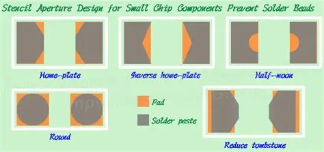
2. Optimize Component Placement for Fine Pitch PCBA
Working with fine pitch PCBA components, such as ball grid arrays (BGAs) with pitches as low as 0.4 mm, is essential for miniaturization. However, tight spacing requires precise placement to avoid misalignment during assembly. Use design software with automated placement tools to ensure components are positioned for optimal signal flow and minimal interference.
Additionally, group related components together to reduce trace lengths. For example, placing a microcontroller near its supporting capacitors can cut trace length by 50%, lowering impedance and improving performance at frequencies above 500 MHz.
3. Use Multi-Layer Boards for Compact Routing
In a compact PCBA layout, single or double-layer boards often fall short. Multi-layer boards (4 to 12 layers or more) provide extra space for routing traces, allowing you to pack more functionality into a smaller area. They also enable dedicated ground and power planes, which reduce EMI—a critical factor in high-density designs.
However, keep in mind that each additional layer increases manufacturing costs by approximately 10-15%. Balance the number of layers with your budget and design needs to achieve cost-effective miniaturization.
4. Incorporate Embedded Components
Embedding passive components like resistors and capacitors directly into the PCB substrate is a powerful PCBA miniaturization technique. This approach frees up surface space for active components and reduces parasitic effects, improving signal integrity. Embedded components can reduce board size by up to 20% in applications like RF modules operating at 2.4 GHz.
While embedding adds complexity to the manufacturing process, the space savings and performance benefits make it a worthwhile investment for high-density designs.
Image Placement Suggestion: Place an image here showing a PCB with embedded components compared to a traditional layout. ALT Text: "PCB with embedded components for PCBA miniaturization."
Advanced PCBA Assembly Techniques for Miniaturization
Designing a high-density board is only half the battle. Advanced PCBA assembly methods are crucial for turning your compact design into a functional product. Here are the key techniques to ensure precision and reliability during assembly.
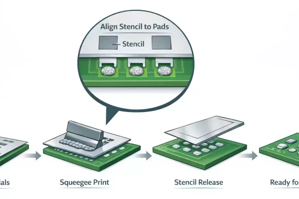
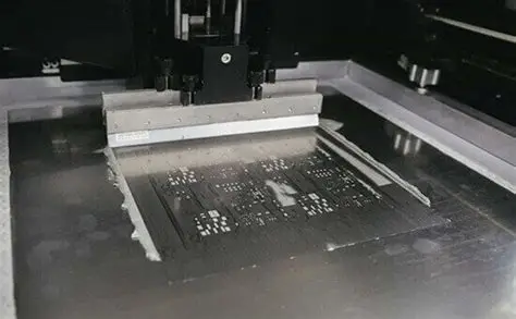
1. Adopt Surface Mount Technology (SMT) with Precision Equipment
Surface Mount Technology (SMT) is the backbone of modern advanced PCBA assembly. SMT allows for smaller components to be mounted directly onto the board’s surface, unlike through-hole technology, which requires more space. Automated pick-and-place machines with placement accuracy of ±0.01 mm are essential for handling fine pitch PCBA components without errors.
For example, assembling a BGA with a 0.4 mm pitch requires precise alignment to avoid bridging or open connections during soldering. Investing in high-quality SMT equipment ensures defect rates remain below 1% even in high-density designs.
2. Use Reflow Soldering for Fine Pitch Components
Reflow soldering is the preferred method for attaching fine pitch PCBA components. This process uses a controlled temperature profile to melt solder paste, creating strong, uniform joints. For fine pitch components, a peak reflow temperature of 245°C and a time above liquidus of 60-90 seconds are typical parameters to ensure reliable bonding without damaging components.
Additionally, use X-ray inspection post-assembly to check for hidden defects like voids in BGA solder joints. This step is critical for maintaining quality in high-density assemblies.
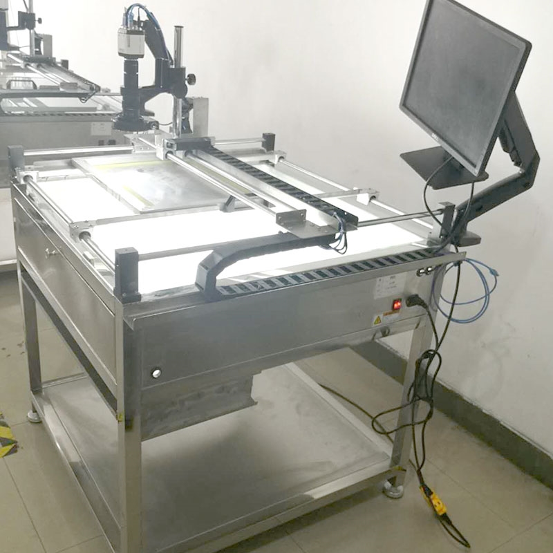
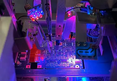
3. Implement Automated Optical Inspection (AOI)
Automated Optical Inspection (AOI) systems are vital for quality control in advanced PCBA assembly. AOI uses high-resolution cameras to detect defects such as misaligned components, missing solder, or incorrect polarity in real time. For high-density boards, AOI can identify issues with components spaced as close as 0.2 mm apart, ensuring reliability before the final product reaches the market.
Image Placement Suggestion: Insert an image here of an AOI machine inspecting a high-density PCBA. ALT Text: "AOI machine inspecting high density PCBA for assembly quality."
Design Tips for Signal Integrity and Thermal Management
Achieving a compact PCBA layout isn’t just about fitting components into a small space. You must also ensure the design performs reliably under real-world conditions. Here are practical tips to address signal integrity and thermal challenges in high-density designs.
1. Minimize Trace Lengths and Impedance Mismatch
Long traces in high-density designs can introduce signal delays and impedance mismatches, especially for signals exceeding 1 GHz. Keep critical traces as short as possible, and match impedance to 50 ohms for RF applications or 100 ohms for differential pairs. Use simulation tools to analyze signal integrity before finalizing your layout.
2. Add Thermal Vias and Heat Sinks
Thermal vias (small holes filled with conductive material) help transfer heat from components to the opposite side of the board or to a heat sink. For a high-power IC generating 5W of heat, placing 10-15 thermal vias with a diameter of 0.3 mm can reduce junction temperature by up to 20°C. Additionally, consider integrating small heat sinks or thermal pads for components in tight spaces.
Tools and Software for High-Density PCBA Design
The right tools can make or break your high density PCBA design efforts. Modern design software offers features like 3D visualization, signal integrity analysis, and automated routing to simplify miniaturization. Look for platforms that support HDI design rules, fine pitch component libraries, and multi-layer stack-up configurations.
Simulation tools are also critical for predicting thermal and electrical performance. For instance, running a thermal simulation can identify hot spots exceeding 85°C, allowing you to adjust your layout before manufacturing.
Image Placement Suggestion: Add an image here showing a screenshot of PCB design software with a high-density layout. ALT Text: "PCB design software displaying high density PCBA layout."
Future Trends in PCBA Miniaturization
The field of PCBA miniaturization techniques is constantly evolving. Emerging trends include 3D packaging, where components are stacked vertically to save space, and the use of advanced materials like flexible substrates for bendable electronics. Additionally, the rise of chiplets—modular semiconductor designs—allows for even greater density by breaking down complex chips into smaller, specialized units.
Staying ahead of these trends ensures your designs remain competitive in a market that demands ever-smaller, more efficient solutions.
Conclusion: Mastering High-Density PCBA Design
Miniaturization is no longer just a trend—it’s a necessity in today’s electronics industry. By adopting high density PCBA design practices, leveraging PCBA miniaturization techniques, and mastering advanced PCBA assembly, you can create compact, powerful devices that meet modern demands. From HDI technology and fine pitch components to thermal management and signal integrity, every aspect of your design and assembly process plays a role in achieving a compact PCBA layout.
Start small by implementing one or two of these strategies in your next project, and gradually build your expertise in fine pitch PCBA and high-density layouts. With the right tools, techniques, and attention to detail, you’ll be well on your way to mastering PCBA miniaturization and delivering innovative solutions that stand out in the market.