 ALLPCB


Introduction
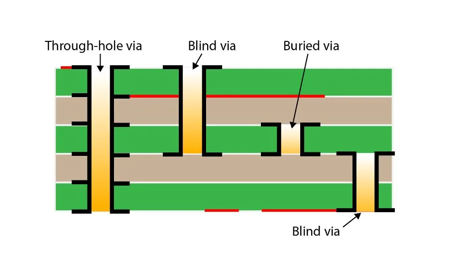
Through-hole vias serve as critical interconnects in printed circuit boards, enabling electrical continuity between layers while supporting component leads in traditional assembly processes. Optimizing through-hole via drill size and via pad size directly influences overall PCB performance, particularly in high-speed designs where signal integrity and impedance control are paramount. Engineers often face challenges in balancing electrical efficiency with mechanical reliability, as suboptimal via dimensions can lead to increased signal loss, crosstalk, or fabrication defects. This article explores the engineering principles behind via sizing, provides structured guidelines for selection, and outlines best practices to enhance PCB performance. By understanding these factors, designers can achieve robust boards that meet stringent performance requirements without compromising manufacturability.
Understanding Through-Hole Via Dimensions and Their Role in PCB Performance
Through-hole vias consist of a drilled hole plated with copper to form a conductive barrel, surrounded by a via pad and annular ring on each layer. The via drill size refers to the diameter of the hole before plating, typically ranging from 0.15 mm to 2.0 mm depending on board thickness and application needs. Via pad size encompasses the copper landing area around the drill hole, which must accommodate the annular ring to ensure plating integrity and mechanical strength. These dimensions collectively determine the via's electrical and thermal characteristics, making them essential for maintaining signal integrity in multilayer boards.
Improper via sizing compromises PCB performance by altering transmission line characteristics and introducing discontinuities. For instance, larger drill sizes reduce copper barrel thickness, potentially increasing resistance and inductance, which degrade high-frequency signals. Conversely, excessively small drills heighten aspect ratio challenges during plating, risking voids or incomplete copper deposition that undermine reliability. In high-speed applications, via pad size affects impedance control, as oversized pads introduce parasitic capacitance that broadens signal rise times and causes reflections. Engineers must therefore prioritize via dimensions that align with layer count, trace widths, and operating frequencies to sustain optimal PCB performance.
The relevance of through-hole via drill size and via pad size extends to manufacturing yields and long-term board reliability. High aspect ratios, defined as board thickness divided by drill diameter, amplify plating difficulties, often leading to barrel cracks under thermal stress. Standards like IPC-2221 provide foundational guidelines for aspect ratios, typically limiting them to 10:1 or less for reliable plating. By optimizing these sizes early in the design phase, teams mitigate risks associated with signal integrity issues, ensuring boards perform consistently across production volumes.
Engineering Principles Governing Via Size Optimization
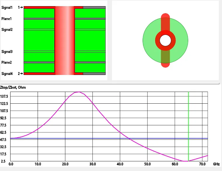
The electrical behavior of through-hole vias stems from their geometry, which introduces inductance, capacitance, and resistance into the signal path. Inductance scales with drill size and via length, following the formula L = (μ? * h) / (2π) * ln(1.27 * D / t), where h is via height, D is average diameter, and t is copper thickness; larger drills thus elevate inductance, disrupting impedance control in controlled-impedance lines. Capacitance arises from the via pad and barrel interacting with adjacent planes or traces, with pad size directly proportional to fringing fields that lower characteristic impedance. Signal integrity suffers when these parasitics cause impedance mismatches, resulting in ringing, overshoot, or eye diagram closure at gigabit speeds.
Thermal management also hinges on via dimensions, as smaller drill sizes with thicker copper walls enhance heat dissipation through the barrel to inner planes. However, this benefit diminishes if plating quality falters due to high aspect ratios, leading to hotspots that accelerate electromigration. Mechanical stress from via drill size influences board warpage and fatigue; oversized drills weaken the laminate structure, while undersized ones concentrate strains at the pad edges during thermal cycling. Engineers model these interactions using field solvers to predict via stub effects in multilayer stacks, where unterminated via lengths beyond a quarter-wavelength become resonant discontinuities.
Impedance control requires precise coordination of via drill size, via pad size, and antipad clearance on reference planes. The transition from trace to via creates a 3D field perturbation, with pad diameters ideally 2.5 to 3 times the drill size to maintain 50-ohm or 100-ohm differentials. Excessive pad expansion disrupts plane shielding, fostering crosstalk between vias spaced closer than three times their pad diameter. These principles underscore the need for simulation-driven optimization, correlating via geometry to time-domain reflectometry measurements for validation.
Best Practices for Selecting Through-Hole Via Drill Size and Via Pad Size
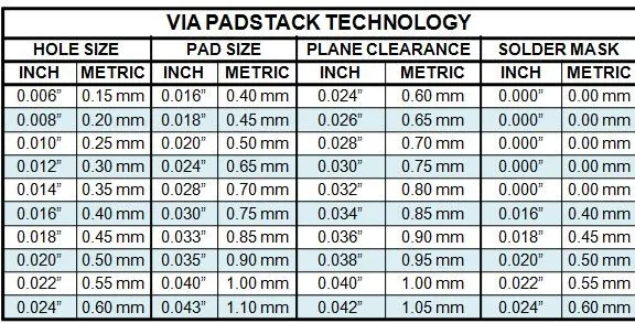
Start via sizing by assessing board thickness and layer count to compute feasible aspect ratios, adhering to IPC-2221 recommendations of 8:1 to 10:1 maximum for standard plating processes. Select the smallest drill size that accommodates lead diameters or supports blind/buried via alternatives, prioritizing 0.3 mm to 0.5 mm for high-density interconnects where signal integrity demands low inductance. Via pad size should feature an annular ring of at least 0.1 mm minimum after plating shrinkage, expanding the pad diameter to drill size plus twice the ring width plus etch factor. This ensures plating overlap and etch tolerance, preventing ring breaks that compromise conductivity.
For impedance-controlled designs, iterate via dimensions in tandem with trace geometry using 2D/3D solvers to target specific Z0 values. Reduce via pad size where possible by tightening antipads on planes, but maintain at least 0.15 mm clearance to avoid shorting during lamination. In power distribution vias, upscale drill sizes modestly to bolster current capacity, calculated via I = k * ΔT^0.44 * A^0.725, where A is cross-sectional copper area, balancing thermal rise with inductance penalties. Validate selections against fabrication capabilities, consulting DFM rules for drill-to-drill spacing at least 2.5 times drill diameter.
Layer stacking influences optimal via profiles; shorter vias in symmetric builds minimize stub effects for better signal integrity. Employ stitching vias around large pads for return current paths, spacing them at λ/20 intervals to suppress slotline modes. Post-design, perform DFT analysis to flag oversized pads contributing to crosstalk budgets exceeding 1% of signal amplitude. These practices elevate PCB performance by integrating electrical, thermal, and mechanical considerations holistically.
Troubleshooting Common Via Sizing Issues in High-Performance PCBs
Engineers frequently encounter signal integrity degradation from via stubs in unterminated through-holes, manifesting as increased insertion loss beyond 5 GHz. Mitigate by back-drilling to remove unused barrel segments, targeting stub lengths under 0.5 mm, or transitioning to microvias for critical nets. Oversized via pads in dense routing can elevate crosstalk; remedy by shrinking pads proportionally while preserving annular rings, verified via S-parameter simulations showing ILD > 30 dB up to Nyquist frequency.
Plating voids from high-aspect via drill sizes appear in cross-sections as laminar cracks, often due to accelerator starvation in electroless copper. Address by relaxing aspect ratios or specifying pulse-reverse electroplating for uniform deposition. IPC-6012 outlines acceptability criteria for barrel quality, mandating void-free walls and minimum plating thickness of 25 μm. Warpage induced by clustered large-drill vias distorts pad coplanarity; counter with balanced via placement and CTE-matched laminates.
Mechanical failures like via pullout during thermal shock testing stem from inadequate annular ring adhesion. Enhance by increasing ring width to 0.15 mm and optimizing surface finish for better Cu-to-laminate bonding. Field returns often trace to these issues, underscoring proactive DFT integration.
Conclusion
Optimizing through-hole via drill size and via pad size forms the cornerstone of superior PCB performance, directly bolstering signal integrity and impedance control. By grounding decisions in engineering principles like inductance scaling and aspect ratio limits, designers sidestep common pitfalls in high-speed and high-reliability applications. Practical guidelines from standards such as IPC-2221 and IPC-6012, coupled with simulation and DFM checks, enable robust implementations. Ultimately, meticulous via sizing not only enhances electrical efficiency but also streamlines manufacturing, yielding boards that excel under real-world stresses. Engineers adopting these structured approaches position their designs for success in evolving PCB demands.
FAQs
Q1: What is the ideal through-hole via drill size for high-speed PCB performance?
A1: Through-hole via drill size should be minimized to reduce inductance while respecting aspect ratios under 10:1 per IPC-2221 guidelines. For signal integrity in gigabit designs, target 0.2 to 0.4 mm drills with corresponding via pad sizes ensuring 50-ohm impedance control. Balance with plating capabilities to avoid voids, simulating parasitics for validation.
Q2: How does via pad size impact signal integrity and impedance control?
A2: Via pad size introduces capacitance that mismatches trace impedance, broadening pulses and causing reflections. Optimal sizing keeps pads 2.5 times drill diameter, minimizing fringing fields while maintaining annular rings. In multilayer boards, this preserves PCB performance by curbing crosstalk in dense routing.
Q3: Why is aspect ratio critical for through-hole via drill size selection?
A3: Aspect ratio, board thickness over drill diameter, governs plating uniformity and reliability. Exceeding 10:1 risks incomplete copper deposition, degrading signal integrity. Select drill sizes to stay within limits, enhancing impedance control and mechanical strength for sustained PCB performance.
Q4: What best practices improve PCB performance through via optimization?
A4: Prioritize smallest feasible drill and pad sizes, model impedance with solvers, and adhere to standards like IPC-6012 for quality. Back-drill stubs, balance via distribution, and verify annular rings to boost signal integrity. These steps ensure robust, high-yield boards.
References
IPC-2221B — Generic Standard on Printed Board Design. IPC, 2012
IPC-6012E — Qualification and Performance Specification for Rigid Printed Boards. IPC, 2017


