 ALLPCB


High-density interconnect printed circuit boards enable the compact, high-performance electronics found in modern devices ranging from smartphones to advanced medical equipment. Engineers and procurement teams often face challenges when moving from standard PCB designs to HDI versions because the finer features demand tighter process controls throughout fabrication and assembly. Understanding these requirements helps teams avoid costly delays and quality issues while meeting performance targets. This guide examines the HDI PCB assembly process from a practical standpoint, focusing on equipment considerations, quality control steps, testing methods, and common defects that arise during production.
What Is HDI PCB Assembly and Why It Matters
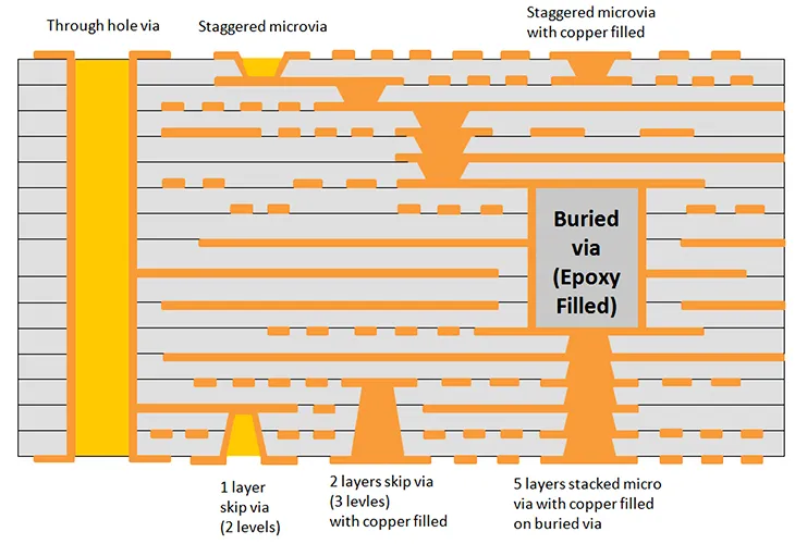
HDI PCB assembly refers to the placement and soldering of components onto boards that incorporate microvias, blind and buried vias, and trace widths or spaces typically below 100 micrometers. These boards support greater component density and shorter signal paths compared with conventional multilayer designs, which improves electrical performance and reduces overall device size. The assembly stage builds on the completed HDI substrate by applying solder paste, positioning parts, and executing reflow or other joining processes under controlled conditions. Industry professionals value HDI technology because it supports the ongoing trend toward miniaturization without sacrificing functionality or reliability in demanding applications.
Technical Principles of HDI PCB Manufacturing Equipment
HDI PCB manufacturing equipment must handle precise via formation and sequential build-up processes that differ from standard PCB production. Laser drilling systems create the small-diameter microvias essential for layer-to-layer connections, while specialized lamination presses apply controlled heat and pressure to bond additional layers without damaging fine features. Pick-and-place machines used in assembly require higher accuracy to align components on pads that may measure only a few hundred micrometers across. Reflow ovens incorporate multiple heating zones and precise thermal profiling to accommodate the thinner copper and resin systems common in HDI constructions. These capabilities collectively allow manufacturers to achieve the interconnect density that conventional equipment cannot reliably support.
The HDI PCB Assembly Process Step by Step
The HDI PCB assembly process begins with solder paste application through a precisely aligned stencil that matches the fine pad geometry. Automated optical inspection follows immediately to verify paste volume and placement before components are positioned by high-precision placement equipment. Reflow soldering then creates the permanent electrical and mechanical connections, with thermal profiles adjusted to accommodate the board's thermal mass and material properties. Subsequent cleaning or conformal coating steps may be added depending on the end-use environment. Throughout these stages, process parameters such as paste viscosity, placement force, and peak temperature must remain within narrow tolerances to prevent defects.
Related Reading: HDI PCB Assembly: Challenges and Best Practices
HDI PCB Quality Control Measures
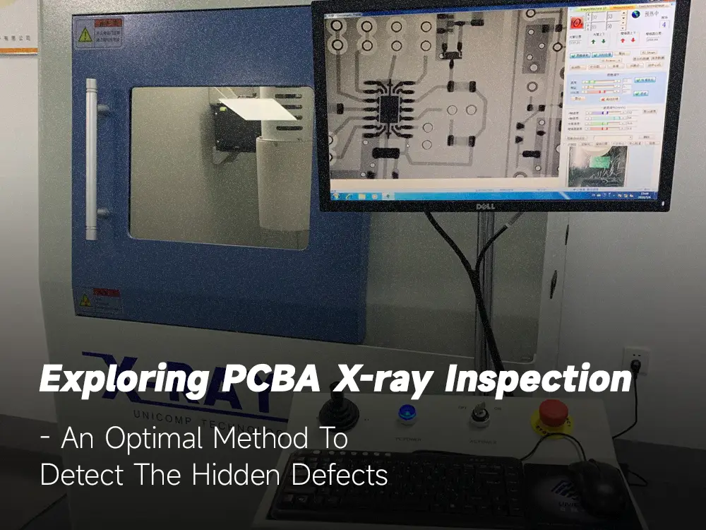
HDI PCB quality control integrates in-process checks and final verification to confirm that assembled boards meet functional and reliability requirements. Automated optical inspection systems scan for visible issues such as misalignment or insufficient solder, while X-ray imaging reveals hidden problems inside microvias or under components. Electrical testing verifies continuity and isolation across the dense interconnect network. These controls align with established industry practices that emphasize consistent process monitoring rather than end-of-line inspection alone. Documentation of each step supports traceability and helps identify trends that could affect future builds.
HDI PCB Testing Methods and Standards
HDI PCB testing combines electrical, mechanical, and environmental evaluations to validate performance under expected operating conditions. In-circuit and functional testing confirm that signals propagate correctly through the fine traces and vias. Thermal cycling and humidity exposure tests assess long-term reliability, particularly for boards that will experience repeated expansion and contraction. Acceptance criteria for these tests draw from recognized specifications that define acceptable limits for voids, delamination, and electrical parameters. Proper test sequencing helps distinguish assembly-related issues from substrate fabrication problems.
Common HDI PCB Assembly Defects and Troubleshooting
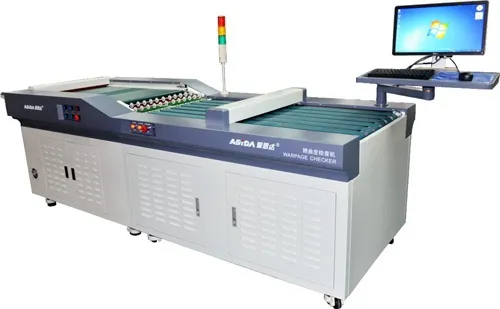
HDI PCB assembly defects often stem from the interaction between fine features and process variables. Microvia voids can occur when plating chemistry or laser parameters leave incomplete copper fill, leading to intermittent connections after thermal stress. Warpage arises when asymmetric copper distribution or mismatched material coefficients cause the board to bend during reflow, complicating component placement and joint formation. Solder bridging becomes more likely on closely spaced pads if paste volume or stencil release is not optimized. Component tombstoning or misalignment frequently results from uneven heating or placement pressure on small pads. Troubleshooting these issues typically involves adjusting one variable at a time, such as reflow profile or stencil design, while monitoring results with targeted inspection.
Best Practices for Reliable HDI PCB Assembly
Best practices emphasize early collaboration between design and manufacturing teams to ensure pad layouts and via placements remain compatible with available equipment capabilities. Maintaining tight control over incoming material moisture levels reduces the risk of delamination during thermal excursions. Regular calibration of placement and inspection equipment preserves the accuracy needed for fine-pitch work. Process capability studies performed on critical steps provide data that guide incremental improvements. When defects appear, root-cause analysis that includes both assembly and substrate variables yields more effective corrective actions than isolated fixes.
Related Reading: HDI Assembly: Achieving High Signal Integrity in Compact Designs
Conclusion
Successful HDI PCB assembly depends on understanding the interplay between substrate characteristics, equipment precision, and process control. Teams that apply structured quality measures and systematic troubleshooting achieve higher yields and more reliable end products. By focusing on the specific requirements of microvias, fine traces, and thermal management, engineers can navigate the added complexity while delivering the compact, high-performance electronics demanded by current markets.
FAQs
Q1: What steps define the HDI PCB assembly process?
A1: The HDI PCB assembly process includes solder paste printing through a fine-feature stencil, high-accuracy component placement, controlled reflow soldering, and post-assembly inspection. Each step requires tighter parameter control than standard PCB assembly because of the smaller pad sizes and microvia structures. Following consistent process documentation helps maintain repeatability across production lots.
Q2: Which equipment supports HDI PCB manufacturing?
A2: HDI PCB manufacturing equipment encompasses laser drilling systems for microvia formation, precision lamination presses, and advanced pick-and-place machines capable of sub-50-micrometer placement accuracy. Reflow ovens with multiple independently controlled zones further ensure uniform heating across thin, dense boards. Selection of equipment must match the target feature sizes and layer counts of the specific design.
Q3: How does HDI PCB quality control differ from standard practices?
A3: HDI PCB quality control incorporates additional X-ray inspection for microvia integrity and higher-resolution automated optical systems to detect issues on fine traces. Electrical testing emphasizes isolation between closely spaced conductors. These enhanced checks, performed at multiple stages, help identify defects that would remain hidden under conventional inspection methods.
Q4: What are typical HDI PCB assembly defects?
A4: Typical HDI PCB assembly defects include microvia voids, board warpage, solder bridging on fine-pitch pads, and component misalignment. These arise from interactions between material properties, thermal profiles, and placement accuracy. Systematic monitoring and adjustment of process variables reduce their occurrence and support higher first-pass yields.





