 ALLPCB


Are you looking to optimize your PCB manufacturing process with multi-board panelization using edge rails? Edge rails are a key element in panel design, offering support and protection during production while ensuring manufacturability. In this comprehensive guide, we’ll dive deep into the essentials of edge rail panel design, manufacturability considerations, design rule checks, and production workflows to help you achieve efficient and cost-effective results. Whether you're a seasoned engineer or just starting out, this detailed walkthrough will provide actionable insights for your next project.
What is Multi-Board Panelization and Why Use Edge Rails?
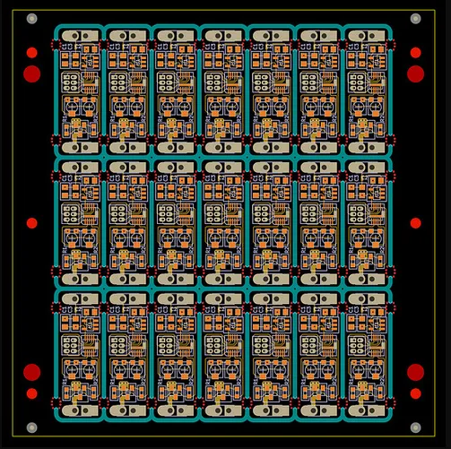
Multi-board panelization is the process of grouping multiple printed circuit boards (PCBs) into a single panel for manufacturing. This technique reduces production costs, streamlines assembly, and maximizes material usage. Edge rails, also known as panel borders or process edges, are non-functional strips of material added around the panel’s perimeter. They serve multiple purposes, such as providing structural stability, protecting board edges during handling, and aiding in automated assembly processes.
Using edge rails in panel design is a smart choice for several reasons. They prevent damage to delicate components near the board edges during depanelization (the process of separating individual boards from the panel). They also offer space for tooling holes and fiducial marks, which are critical for precise alignment during manufacturing. By incorporating edge rails, you can enhance the overall manufacturability of your design and reduce the risk of errors in production.
Key Elements of Edge Rail Panel Design
Designing a panel with edge rails requires careful planning to ensure compatibility with manufacturing equipment and processes. Below are the critical aspects to focus on during the edge rail panel design phase:
1. Edge Rail Width and Spacing
The width of edge rails typically ranges from 5 mm to 10 mm, depending on the manufacturing requirements and the size of the panel. A wider edge rail provides more stability but consumes additional material, increasing costs. Conversely, a narrower rail saves material but may not offer sufficient protection or space for tooling features. As a general rule, consult with your manufacturing partner to confirm the minimum edge rail width for their equipment—most standard processes accommodate a 7 mm rail.
Spacing between individual boards within the panel is equally important. Maintain at least 2-3 mm of clearance between boards to allow for clean separation during depanelization, whether using V-scoring or tab-routing methods. Insufficient spacing can lead to damage or jagged edges on the final boards.
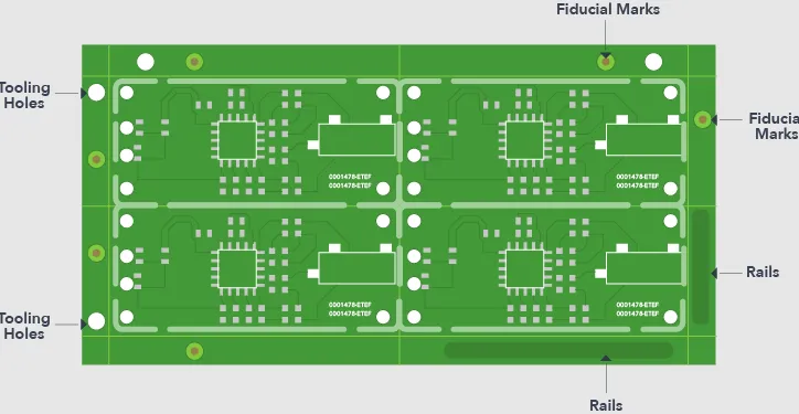
2. Tooling Holes and Fiducial Marks
Edge rails often serve as the location for tooling holes and fiducial marks. Tooling holes, usually 3.2 mm in diameter, are used to secure the panel during manufacturing and assembly. Place at least three tooling holes on the edge rails (one in each corner) to ensure stability. Fiducial marks, small copper dots typically 1 mm in diameter, assist in aligning the panel during automated processes like pick-and-place assembly. Position these marks on the edge rails, away from active board areas, to avoid interference with functional components.
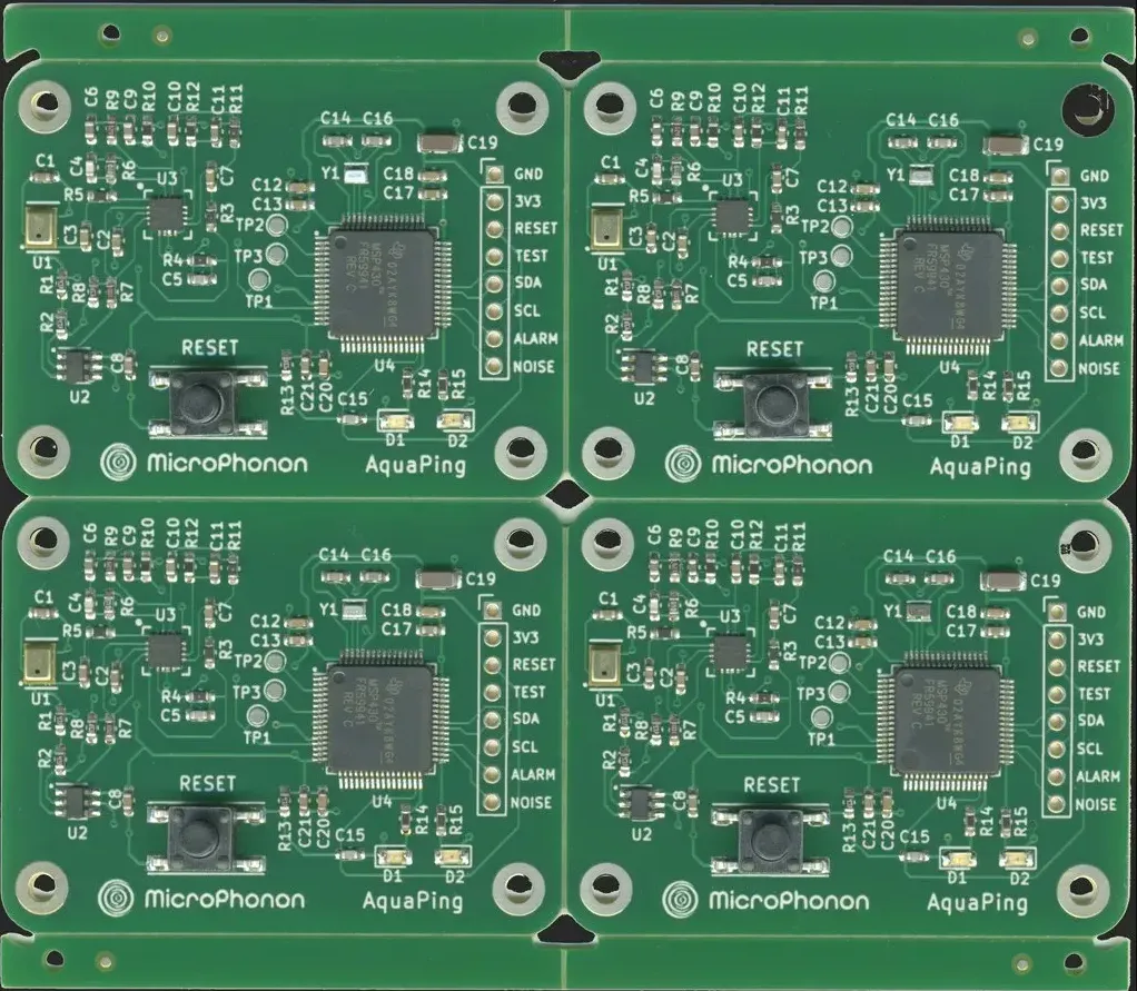
3. Breakaway Tabs or V-Scoring
Edge rails connect to individual boards via breakaway tabs or V-scores. Breakaway tabs are small, perforated connections that allow manual separation after assembly. Design these tabs to be 0.5-1 mm thick to balance ease of separation with structural integrity during production. V-scoring, on the other hand, involves cutting shallow grooves (typically 0.3 mm deep) along the separation lines for cleaner, automated depanelization. Choose the method based on your project’s needs—V-scoring is ideal for high-volume production, while tabs suit smaller runs.
Manufacturability Considerations for Edge Rail Panelization
Designing a panel with edge rails is only half the battle; ensuring manufacturability is equally critical. Here are key considerations to keep in mind to avoid delays and costly redesigns during production:
1. Material Selection and Panel Size
The material used for edge rails should match the PCB substrate, typically FR-4 with a thickness of 1.6 mm for standard designs. Mismatched materials can cause uneven stress during manufacturing, leading to warping or cracking. Additionally, consider the overall panel size—most manufacturers support panels up to 500 mm x 400 mm, but larger panels may require special handling, increasing costs. Optimize your panel layout to fit within standard dimensions while maximizing the number of boards per panel.
2. Component Placement Near Edges
Avoid placing sensitive components closer than 5 mm to the board edges. During depanelization, mechanical stress from cutting or breaking can damage components or traces near the separation lines. If components must be placed near edges due to design constraints, ensure the edge rails are wide enough to absorb stress and protect the active areas.
3. Thermal and Mechanical Stress
Edge rails help distribute thermal and mechanical stress during soldering and assembly. For high-density designs with heavy components, wider edge rails (around 10 mm) can prevent panel bowing under heat or weight. Additionally, ensure that the panel design accounts for thermal expansion—leave small gaps (0.2-0.3 mm) in breakaway tabs to accommodate material expansion during reflow soldering, which can reach temperatures up to 260°C.
Design Rule Check (DRC) for Edge Rail Panelization
A thorough design rule check (DRC) is essential to catch potential issues before sending your panel design to manufacturing. DRC ensures that your design adheres to the manufacturer’s capabilities and industry standards. Here’s how to approach DRC for edge rail panelization:
1. Verify Edge Rail Dimensions
Use your design software to confirm that edge rail widths and board spacing meet the minimum requirements (e.g., 5-7 mm for rails and 2-3 mm between boards). Most modern PCB design tools allow you to set custom rules to flag violations automatically. Double-check that tooling holes are correctly sized (3.2 mm) and positioned in non-functional areas of the edge rails.
2. Check for Overlapping Features
Ensure that no traces, vias, or components overlap with breakaway tabs or V-score lines. Overlapping features can result in damaged boards or electrical failures after depanelization. Set a clearance rule of at least 1.5 mm around separation lines to keep critical elements safe.
3. Validate Panel Strength
Run a simulation or manual check to ensure the panel remains structurally sound during handling. For instance, a panel with insufficient edge rail width or poorly placed tooling holes may crack under mechanical stress. If your design software supports stress analysis, use it to identify weak points and adjust the edge rail design accordingly.
Production Workflow for Multi-Board Panelization with Edge Rails
Understanding the production workflow helps you design panels that align with manufacturing processes. Here’s a step-by-step overview of how edge rails fit into the production pipeline:
1. Panel Layout Finalization
Once your design passes DRC, finalize the panel layout by arranging multiple boards within the panel boundaries. Use edge rails to frame the panel, ensuring symmetry for balanced stress distribution. Export the panel design as a Gerber file, including a separate layer for edge rails and separation lines to guide the manufacturer.
2. Fabrication and Assembly
During fabrication, the manufacturer uses the edge rails for handling and alignment. Tooling holes secure the panel to CNC machines for drilling and routing, while fiducial marks guide automated assembly equipment. Edge rails also protect the panel during soldering processes, such as wave soldering, which can apply significant thermal stress.
3. Depanelization and Testing
After assembly, individual boards are separated from the panel using the designated breakaway tabs or V-scores. Edge rails are discarded or recycled, having served their purpose of protection and alignment. Finally, each board undergoes electrical testing to ensure functionality—proper edge rail design minimizes the risk of damage during this final stage.
Best Practices for Optimizing Edge Rail Panel Design
To wrap up, here are some best practices to ensure your edge rail panel design is efficient and manufacturable:
- Collaborate Early: Work closely with your manufacturing partner during the design phase to confirm edge rail specifications and panel constraints.
- Minimize Waste: Arrange boards in a way that maximizes panel usage while maintaining adequate edge rail width and spacing.
- Test Iteratively: For complex designs, prototype a small panel run to identify potential issues with edge rails or depanelization before full-scale production.
- Document Clearly: Include detailed notes in your design files about edge rail dimensions, separation methods, and tooling hole placements to avoid miscommunication with the manufacturer.
Conclusion
Multi-board panelization with edge rails is a powerful strategy to enhance the efficiency and reliability of PCB manufacturing. By focusing on edge rail panel design, manufacturability considerations, design rule checks, and production workflows, you can create panels that reduce costs, protect your boards, and streamline the production process. Remember to prioritize proper spacing, tooling features, and stress management in your designs to achieve the best results. With the insights provided in this guide, you’re well-equipped to tackle your next panelization project with confidence and precision.
At ALLPCB, we’re committed to supporting engineers with resources and expertise to optimize every stage of PCB design and manufacturing. Apply these edge rail panelization tips to your workflow and experience smoother, more cost-effective production runs.


