ALLPCB


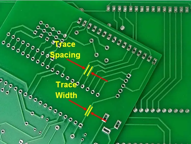
Trace spacing and width decisions directly influence the electrical performance, thermal behavior, and long-term reliability of printed circuit boards. Engineers working on power electronics, industrial controls, and high-voltage assemblies frequently turn to online calculators to determine appropriate dimensions quickly. These tools draw from established guidelines to suggest minimum clearances and conductor widths based on voltage, current, and environmental factors. While convenient, they also introduce risks when users treat outputs as absolute without deeper validation.
The Role of Trace Spacing and Width in Reliable PCB Performance
Proper trace spacing prevents unintended electrical conduction between conductors, which can lead to arcing, short circuits, or insulation breakdown under voltage stress. Trace width, meanwhile, determines the current-carrying capacity of each conductor before excessive heating occurs. Inadequate spacing or undersized traces can compromise safety margins, especially in environments with high humidity, contamination, or temperature fluctuations. Electric engineers must balance these factors against board size constraints, signal integrity needs, and manufacturing capabilities. Overly conservative spacing wastes real estate, while insufficient dimensions invite field failures.
Foundations in Industry Standards for Calculation Methods
Design guidelines for conductor spacing and sizing originate from systematic testing of insulation performance and thermal dissipation across various board constructions. IPC-2221 provides the primary framework for determining minimum electrical clearances based on voltage levels and operating conditions. This standard accounts for factors such as uncoated versus coated surfaces and internal versus external layers. Complementary documents address current-carrying capacity more specifically through empirical data on temperature rise. Engineers reference these resources to establish baseline requirements before applying any computational aids.
Capabilities and Shortcomings of Online Trace Calculators
A pcb trace spacing calculator online or ipc 2221 calculator can accelerate initial layout iterations by applying standard tables or formulas to user-supplied voltage and current values. High voltage pcb calculator tools extend this utility to applications involving hundreds or thousands of volts, where creepage and clearance distances become critical. Trace width calculator functions similarly help size power traces to limit temperature rise within acceptable limits. These resources promote consistency and reduce manual lookup time during early design phases.
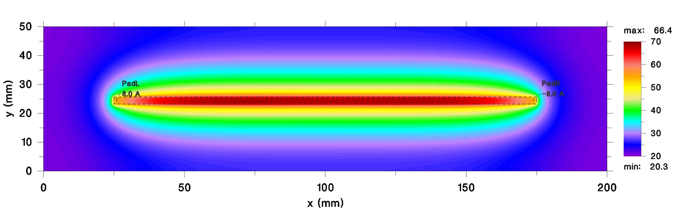
However, calculators rely on simplified models that may not capture every real-world variable. Input errors, such as incorrect assumptions about coating thickness or altitude derating, propagate directly into outputs. Manufacturing tolerances, material variations, and assembly processes can alter actual performance compared with idealized predictions. Over-reliance without cross-verification risks boards that pass simulation yet fail qualification testing or field operation.
Effective Integration of Calculators into the Design Workflow
Begin by confirming that calculator inputs align precisely with the intended operating environment, including maximum voltage, continuous current, ambient temperature range, and pollution degree. Cross-check results against the underlying standard tables rather than accepting single-point outputs. Incorporate margin for manufacturing variations and perform thermal modeling or prototype measurements on critical nets. Combine calculator guidance with design rule checks in layout software and physical testing under worst-case conditions. This layered approach preserves the speed advantage while mitigating blind spots.
Practical Considerations for High-Voltage and Power Applications
High-voltage designs demand particular attention to both clearance (line-of-sight distance) and creepage (distance along the surface) to prevent flashover. Calculators provide starting points, yet engineers must also evaluate surface finish, solder mask quality, and potential contamination sources. Power traces require simultaneous evaluation of width for heating and spacing for isolation, often leading to iterative adjustments. Documentation of assumptions and verification steps supports traceability during design reviews and regulatory submissions.
Conclusion
Trace spacing and width calculators serve as efficient aids when grounded in sound engineering judgment and standard-based validation. They streamline routine tasks yet cannot replace comprehensive understanding of electrical, thermal, and environmental influences. Consistent application of best practices, including input verification, cross-referencing with IPC-2221, and empirical confirmation, yields designs that meet performance targets reliably. Electric engineers who maintain this balance achieve both productivity and robustness in their PCB layouts.
FAQs
Q1: How does a pcb trace spacing calculator online assist with high-voltage designs?
A1: It applies established clearance and creepage recommendations to input voltage levels, helping engineers establish initial spacing values that align with safety requirements while allowing quick exploration of layout options.
Q2: What role does an ipc 2221 calculator play in determining trace dimensions?
A2: The calculator references the generic design standard to suggest minimum conductor spacing and related parameters based on voltage, coating status, and layer location, providing a consistent starting point for compliance-oriented layouts.
Q3: When should a high voltage pcb calculator be supplemented with additional analysis?
A3: Additional analysis becomes necessary when designs involve unusual environmental conditions, non-standard materials, or tight mechanical constraints that fall outside the simplified assumptions built into most calculator models.
Q4: How does a trace width calculator relate to overall board reliability?
A4: It estimates conductor sizes needed to carry specified currents without excessive temperature rise, contributing to thermal management and long-term electrical integrity when combined with proper spacing considerations.