 ALLPCB


In the fast-paced world of electronics, high-speed PCB design is critical for ensuring devices perform reliably. But with higher speeds come significant challenges, especially when it comes to maintaining signal integrity. If you're struggling with issues like signal distortion, crosstalk, or reflections in your designs, you're not alone. This blog will guide you through mastering high-speed PCB signal integrity by addressing common problems and offering practical solutions like impedance matching, crosstalk reduction, and troubleshooting signal reflections.
Whether you're designing for telecommunications, computing, or IoT devices, understanding how to tackle these challenges is key to creating robust and efficient PCBs. Let’s dive into the details of high-speed PCB design, explore the root causes of signal integrity issues, and provide actionable tips to overcome them using the right techniques and high-frequency PCB materials.
What Is High-Speed PCB Design and Why Does Signal Integrity Matter?
High-speed PCB design refers to creating printed circuit boards that operate at high frequencies, typically above 50 MHz, where signal timing and quality become critical. At these speeds, even small design flaws can lead to data errors, delays, or complete system failures. Signal integrity (SI) is the measure of how well a signal maintains its quality as it travels through the PCB. Poor SI can result in distorted signals, affecting the performance of devices like smartphones, servers, or medical equipment.
Maintaining high-speed PCB signal integrity is vital because it ensures data is transmitted accurately and without interference. As frequencies increase, challenges like signal reflection, crosstalk, and electromagnetic interference (EMI) become more pronounced. By addressing these issues early in the design process, you can avoid costly redesigns and ensure your product meets performance expectations.

Key Signal Integrity Challenges in High-Speed PCB Design
Designing for high speeds means confronting several obstacles that can degrade signal quality. Below, we break down the most common signal integrity challenges and explain why they occur.
1. Signal Reflections Due to Impedance Mismatches
Signal reflection happens when a signal encounters a change in impedance along its path, causing part of the signal to bounce back. This can distort the original signal and lead to errors. For example, if a trace on a PCB designed for 50 ohms impedance connects to a component with a different impedance, reflections are likely to occur. At high frequencies, even a mismatch of a few ohms can cause significant issues.
To put this into perspective, a signal traveling at 1 GHz can experience reflection issues if the impedance varies by more than 10%. This is why impedance matching in PCB design is non-negotiable for high-speed applications.
2. Crosstalk Between Adjacent Traces
Crosstalk occurs when signals on nearby traces interfere with each other due to electromagnetic coupling. This is especially problematic in high-speed designs where traces are often placed close together to save space. For instance, if two traces carrying signals at 2.5 GHz are spaced only 5 mils apart without proper shielding, crosstalk can introduce noise, leading to data corruption.
Reducing crosstalk in high-speed PCBs requires careful planning of trace spacing and the use of ground planes to minimize interference.
3. Electromagnetic Interference (EMI)
EMI is unwanted noise from external or internal sources that disrupts signal quality. In high-speed designs, fast-switching signals can generate EMI, affecting nearby components or even other devices. For example, a poorly grounded PCB operating at 5 GHz might radiate noise that interferes with a nearby wireless module.
Proper grounding and shielding techniques are essential to control EMI and maintain signal integrity.
4. Signal Loss Due to High-Frequency Effects
At high frequencies, signals can lose strength due to dielectric losses in the PCB material and skin effect in conductors. For instance, a signal at 10 GHz traveling through a standard FR-4 material might lose up to 20% of its amplitude over a 10-inch trace due to material properties. This loss can degrade performance, especially in long-distance data transmission.
Choosing the right high-frequency PCB materials is crucial to minimize these losses.
Practical Solutions for Overcoming Signal Integrity Challenges
Now that we’ve identified the key challenges, let’s explore practical strategies to address them. These solutions are designed to help you achieve reliable performance in your high-speed PCB projects.
Impedance Matching in PCB Design: Getting It Right
Impedance matching ensures that the impedance of traces, components, and terminations are aligned to prevent signal reflections. Here are some tips to achieve proper impedance matching:
- Calculate Trace Impedance: Use tools or formulas to design traces with specific impedance values. For example, a 50-ohm trace on a 1.6mm thick board with a dielectric constant of 4.5 might require a width of 2.8mm. Adjust based on your stack-up and material.
- Use Termination Resistors: Adding resistors at the end of a transmission line can absorb reflected signals. For a 50-ohm line, a 50-ohm resistor can significantly reduce reflections.
- Controlled Impedance Routing: Work with your manufacturer to ensure traces are fabricated to meet the target impedance within a tolerance of ±10%.
By prioritizing impedance matching in PCB design, you can minimize reflections and ensure cleaner signal transmission.
Reducing Crosstalk in High-Speed PCBs: Layout Tips
Crosstalk can be a major issue, but with the right layout techniques, it’s manageable. Consider these strategies for reducing crosstalk in high-speed PCBs:
- Increase Trace Spacing: Maintain a spacing of at least 3 times the trace width between high-speed signals. For example, if your trace is 5 mils wide, keep a 15-mil gap to reduce coupling.
- Use Ground Planes: Place a solid ground plane beneath signal layers to act as a shield. This can reduce crosstalk by up to 50% in densely packed designs.
- Route Signals on Different Layers: If spacing is limited, route critical signals on separate layers with ground planes in between to isolate them.
These practices can significantly lower interference and improve overall signal quality.
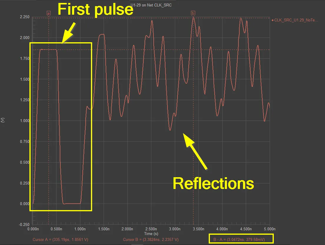
Signal Reflection Troubleshooting: Identifying and Fixing Issues
If you’re already facing signal reflection problems in your design, troubleshooting is the next step. Here’s how to identify and resolve these issues:
- Use Simulation Tools: Software can simulate signal behavior and highlight impedance mismatches. Look for reflections in the waveform that indicate a problem.
- Check Termination: Ensure termination resistors match the trace impedance. A mismatch as small as 5 ohms can cause noticeable reflections at 1 GHz.
- Inspect Vias and Connectors: Vias and connectors can introduce impedance discontinuities. Minimize via usage or use back-drilling to reduce stub effects.
Signal reflection troubleshooting requires patience and precision, but addressing these issues can save your design from performance bottlenecks.
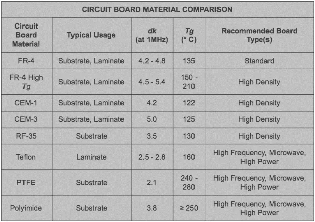
Choosing High-Frequency PCB Materials for Optimal Performance
The choice of material plays a huge role in managing signal loss and maintaining integrity at high frequencies. Standard materials like FR-4 might work for low-speed designs, but they fall short above 1 GHz due to high dielectric losses. Here are some considerations for selecting high-frequency PCB materials:
- Low Dielectric Constant (Dk): Materials with a Dk below 3.5, such as PTFE-based laminates, reduce signal delay and loss. For example, a material with a Dk of 2.2 can improve signal speed by 15% compared to FR-4.
- Low Dissipation Factor (Df): A Df below 0.002 minimizes energy loss. This is critical for signals above 5 GHz, where losses can exceed 30% with standard materials.
- Thermal Stability: High-frequency materials should withstand temperature changes without altering their electrical properties, ensuring consistent performance.
Investing in the right high-frequency PCB materials can make a significant difference in signal integrity, especially for applications like 5G or radar systems.
Advanced Techniques for High-Speed PCB Design
Beyond the basics, there are advanced techniques that can further enhance signal integrity in your designs. These methods require more expertise but offer substantial benefits for cutting-edge applications.
Differential Pair Routing for Noise Immunity
Differential pairs involve routing two traces carrying complementary signals to cancel out noise. This technique is common in high-speed interfaces like USB or PCIe. Keep the traces equal in length (within 5 mils) and maintain consistent spacing to ensure the signals arrive simultaneously.
Minimizing Via Stubs with Back-Drilling
Via stubs are unused portions of vias that can act as antennas, causing reflections. Back-drilling removes these stubs, improving signal quality. For a design operating at 10 GHz, back-drilling can reduce signal loss by up to 10%.
Power Distribution Network (PDN) Optimization
A stable power supply is crucial for high-speed designs. Use decoupling capacitors close to power pins (within 100 mils) and design low-impedance power planes to minimize noise. A well-optimized PDN can reduce power supply noise by 20-30%, directly improving signal integrity.
Conclusion: Building Better High-Speed PCBs
Mastering high-speed PCB design is all about overcoming signal integrity challenges with the right techniques and materials. By focusing on impedance matching in PCB design, reducing crosstalk in high-speed PCBs, and using high-frequency PCB materials, you can ensure your designs perform reliably even at the highest frequencies. Signal reflection troubleshooting and advanced methods like differential pair routing further enhance your ability to tackle complex projects.
At ALLPCB, we’re committed to supporting your high-speed design journey with top-notch manufacturing capabilities and expert guidance. Whether you’re working on a 5G application or a high-performance computing board, applying these principles will help you achieve success. Start implementing these strategies in your next project and experience the difference in performance and reliability.


