 ALLPCB


If you're looking for a way to enhance your printed circuit board (PCB) designs, understanding PCB copper pour is essential. Copper pour, also known as copper fill or copper flooding, involves filling unused areas of a PCB with solid copper, typically connected to ground or power nets. This technique can improve signal integrity, aid in thermal management, and reduce electromagnetic interference (EMI). In this ultimate guide, we’ll dive deep into the benefits, design tips, and best practices for using copper pour to optimize your PCB layouts for performance and reliability.
What Is PCB Copper Pour and Why Does It Matter?
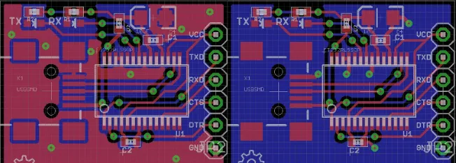
Copper pour refers to the process of covering empty spaces on a PCB layer with a solid layer of copper. This copper is often tied to a specific net, such as ground (GND) or a power supply (VCC), to create a uniform plane. The primary purpose of copper pour is to provide a low-impedance path for current, reduce noise, and improve the overall stability of the circuit.
Why does it matter? Without proper copper pour, your PCB might suffer from inconsistent signal return paths, increased EMI, and poor heat dissipation. For high-speed designs or circuits operating in harsh environments, these issues can lead to performance degradation or even failure. By implementing copper pour effectively, you can address these challenges and create more robust designs.
Key Benefits of Using Copper Pour in PCB Design
Let’s explore the major advantages of incorporating copper pour into your PCB designs. These benefits directly impact signal integrity, thermal management, and overall board performance.
1. Improved Signal Integrity
Signal integrity is critical for high-speed circuits where data rates can exceed several gigabits per second. Copper pour, especially when connected to ground, creates a consistent reference plane for signals. This minimizes impedance mismatches and reduces crosstalk between adjacent traces. For example, in a 5 GHz signal application, a well-designed ground plane can lower return loss by up to 10 dB compared to a board without a solid plane.
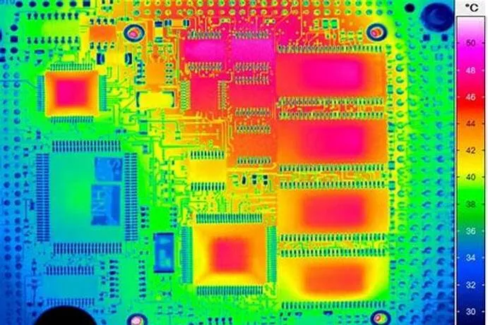
2. Enhanced Thermal Management
Heat dissipation is a common challenge in PCB design, especially for power electronics. Copper pour acts as a heat sink, spreading thermal energy across the board and preventing hotspots. A study on thermal performance showed that a PCB with a copper pour can reduce peak temperatures by 15-20°C under high-load conditions compared to a board without it.
3. Reduced Electromagnetic Interference (EMI)
EMI can disrupt circuit operation and cause compliance issues. A solid copper plane helps shield sensitive signals from external noise and confines high-frequency currents to specific paths, reducing radiation. This is particularly important for designs that must meet strict regulatory standards like FCC or CE.
4. Simplified Manufacturing Process
Copper pour can balance the copper distribution on a PCB, reducing the risk of warping during manufacturing. Even copper coverage ensures uniform etching and plating, leading to fewer defects and higher yield rates.
Design Tips for Effective PCB Copper Pour
While copper pour offers numerous benefits, improper implementation can lead to issues like increased capacitance or unintended short circuits. Here are actionable design tips to ensure you get the most out of copper pour in your layouts.
1. Connect Copper Pour to the Right Net
Always tie your copper pour to a specific net, typically ground or power. Leaving it floating (unconnected) can create a large antenna, amplifying EMI instead of reducing it. For multi-layer boards, ensure the ground plane on each layer connects through vias to maintain continuity.
2. Maintain Proper Clearance Around Components and Traces
Set appropriate clearance rules between copper pour and other elements like traces, pads, and component footprints. A common clearance value is 0.2 mm (8 mils) for low-voltage designs, but this may increase to 0.5 mm (20 mils) or more for high-voltage applications to prevent arcing.
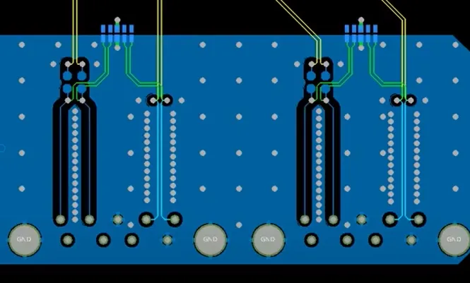
3. Use Via Stitching for Multi-Layer Boards
In multi-layer designs, via stitching connects copper pours on different layers, creating a low-impedance path for return currents. Place vias at regular intervals (e.g., every 10-15 mm) along the edges of the pour to minimize signal loop areas and improve EMI performance.
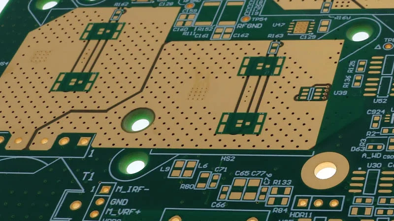
4. Avoid Copper Pour Under High-Frequency Components
For components like RF antennas or high-speed oscillators, avoid placing copper pour directly beneath them. The added capacitance from the copper can detune the circuit or alter signal characteristics. Instead, create a keep-out zone under such components.
5. Balance Copper Distribution
Uneven copper distribution can cause mechanical stress during fabrication, leading to board warping. If one side of the PCB has a large copper pour and the other does not, consider adding dummy copper fills on the less dense side to achieve balance.
Signal Integrity: How Copper Pour Plays a Role
Signal integrity ensures that electrical signals travel through the PCB without distortion or loss. Copper pour is a key factor in maintaining signal quality, especially for high-speed digital and analog designs.
Creating a Low-Impedance Return Path
High-speed signals require a consistent return path to avoid reflections and signal degradation. A solid ground plane created by copper pour provides this path, reducing loop inductance. For instance, at 1 GHz, a signal traveling over a solid ground plane might experience a loop inductance of less than 1 nH, compared to 5-10 nH without it.
Reducing Crosstalk
Crosstalk occurs when signals on adjacent traces interfere with each other. A copper pour tied to ground acts as a shield, absorbing stray electromagnetic fields and minimizing coupling. Spacing traces at least 3 times the trace width apart, combined with a ground plane, can reduce crosstalk by up to 50%.
Managing Impedance Control
For controlled impedance traces, such as those used in USB or HDMI interfaces, copper pour ensures a stable dielectric environment. This helps maintain target impedance values (e.g., 50 ohms for single-ended signals) within a tight tolerance of ±10%.
Thermal Management with Copper Pour: Best Practices
Effective thermal management extends the lifespan of your PCB and prevents component failure. Copper pour is a powerful tool for dissipating heat, but it must be used strategically.
1. Maximize Copper Area Near Heat-Generating Components
Place copper pour close to power components like voltage regulators or high-current ICs. A larger copper area can dissipate heat more effectively. For example, a 2 oz copper layer can handle up to 50% more thermal load than a 1 oz layer under similar conditions.
2. Add Thermal Vias for Heat Transfer
Thermal vias connect copper pours on different layers, allowing heat to transfer from the top to the bottom of the board. A grid of thermal vias (e.g., 0.3 mm diameter, spaced 1.2 mm apart) under a high-power component can reduce its junction temperature by 10-15°C.
3. Use Copper Pour with Heat Sinks
If your design includes heat sinks, extend the copper pour to connect directly with the heat sink mounting area. This creates a direct thermal path, improving heat dissipation efficiency by up to 30% in some cases.
4. Avoid Isolating Copper Islands
Small, disconnected copper areas can trap heat and create hotspots. Ensure all copper pour regions are connected to a larger plane or net to distribute thermal energy evenly across the board.
Common Mistakes to Avoid with PCB Copper Pour
Even with the best intentions, mistakes in copper pour implementation can lead to design flaws. Here are some pitfalls to watch out for.
1. Ignoring Clearance Violations
Failing to set proper clearance between copper pour and other elements can result in short circuits or manufacturing defects. Always double-check design rule checks (DRC) in your layout software to catch these issues early.
2. Overusing Copper Pour
While copper pour is beneficial, covering every inch of the PCB isn’t always necessary. Excessive pour can increase parasitic capacitance, affecting high-frequency signals. Use it only where it adds value, such as under noisy or high-speed areas.
3. Neglecting Ground Plane Continuity
Split ground planes or poorly placed vias can disrupt return paths, leading to signal integrity issues. Ensure your copper pour forms a continuous plane without unnecessary breaks or slots.
Advanced Considerations for Copper Pour in Complex Designs
For advanced PCB designs, such as those in RF or high-power applications, copper pour requires additional attention.
RF Design Considerations
In RF circuits, copper pour must be carefully managed to avoid altering the characteristic impedance of transmission lines. Use coplanar waveguide structures with ground pour on the same layer to maintain signal integrity at frequencies above 1 GHz.
High-Power Applications
For high-power designs, thicker copper layers (e.g., 2 oz or 3 oz) combined with wide pour areas can handle currents exceeding 10 A without overheating. Calculate the required copper thickness using current density guidelines (typically 0.5 A per square mil for 1 oz copper).
Conclusion: Elevate Your PCB Designs with Copper Pour
PCB copper pour is a powerful technique for improving signal integrity, enhancing thermal management, and reducing EMI in your designs. By following the design tips and best practices outlined in this guide, you can optimize your layouts for performance and reliability. Whether you’re working on a simple hobbyist project or a complex high-speed board, copper pour can make a significant difference in the quality of your final product.
Start implementing these strategies in your next design to see the benefits firsthand. From maintaining proper clearances to using thermal vias, every detail counts in creating a robust and efficient PCB. With this ultimate guide to PCB copper pour, you’re equipped to take your designs to the next level.


