 ALLPCB


When it comes to designing a printed circuit board (PCB), choosing the right vias is crucial for ensuring optimal performance, signal integrity, and manufacturability. Vias are small conductive pathways that connect different layers of a PCB, and selecting the appropriate type can make or break your design. Whether you're working on a simple prototype or a complex high-speed circuit, understanding via types in PCB design—such as through-hole vias, blind vias, buried vias, and microvias—along with techniques like via stitching and via size guidelines, can significantly impact your project’s success.
In this comprehensive guide, we'll walk you through the essentials of selecting the right vias for your PCB design. You'll learn about the different types of vias, how to minimize via inductance, and best practices for improving signal integrity with vias. Let's dive into the details to help you achieve a high-performing and reliable PCB design.
What Are Vias in PCB Design and Why Do They Matter?
Vias are tiny holes in a PCB that are plated with conductive material, usually copper, to create electrical connections between different layers of the board. They are essential for routing signals, power, and ground across multilayer designs. Without vias, it would be impossible to create compact, complex circuits that modern electronics demand.
The importance of vias goes beyond just connectivity. Poorly designed or incorrectly chosen vias can lead to signal degradation, electromagnetic interference (EMI), and even manufacturing issues. By understanding via types in PCB design and following best practices, you can ensure your board performs efficiently and reliably in its intended application.
Understanding Via Types in PCB Design
Not all vias are created equal. Depending on your design requirements, you may need to choose between several types of vias. Let's explore the most common options and their specific uses.
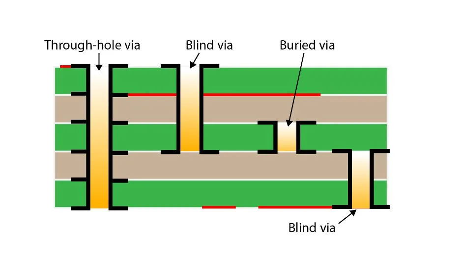
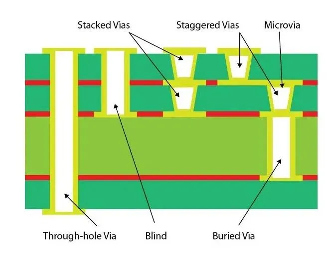
1. Through-Hole Vias
Through-hole vias are the most traditional and widely used type. These vias extend through the entire thickness of the PCB, connecting the top layer to the bottom layer and any layers in between. They are typically larger in diameter (often 0.3mm to 1mm) and are easy to manufacture, making them cost-effective for simpler designs.
However, through-hole vias can take up valuable space on all layers, which may not be ideal for high-density designs. They are best suited for low-frequency applications or boards where space is not a constraint.
2. Blind Vias
Blind vias connect an outer layer (top or bottom) to an inner layer but do not extend through the entire board. For example, a blind via might connect the top layer to the second layer without reaching the bottom. These vias are useful for high-density interconnect (HDI) designs where space is limited, as they free up real estate on the opposite side of the board.
Blind vias are more complex to manufacture than through-hole vias, which can increase costs. They are often used in compact devices like smartphones and wearables.
3. Buried Vias
Buried vias are located entirely within the inner layers of a PCB and do not reach the outer surfaces. For instance, a buried via might connect layer 2 to layer 3 in a six-layer board without touching the top or bottom layers. These vias are ideal for HDI designs because they maximize space on the outer layers for components and traces.
Like blind vias, buried vias are more expensive to produce due to the precision required during manufacturing. They are commonly found in advanced electronics where multilayer routing is critical.
4. Microvias
Microvias are small-diameter vias (typically less than 0.15mm) used in HDI designs. They are often created using laser drilling, which allows for precise placement and minimal space usage. Microvias can be blind or buried and are essential for modern, compact electronics with fine-pitch components like ball grid arrays (BGAs).
While microvias enable high-density designs, they can be challenging to manufacture reliably and may increase production costs. They are best used when space and signal integrity are top priorities.
Via Stitching: Enhancing Grounding and EMI Control
Via stitching is a technique where multiple vias are placed close together to connect ground planes or power planes across layers. This method creates a low-impedance path for return currents, reducing electromagnetic interference (EMI) and improving signal integrity with vias.
Via stitching is particularly important in high-speed designs where ground loops or noise can degrade performance. For example, in a PCB operating at frequencies above 1 GHz, stitching vias spaced at intervals of 1/10th of the wavelength (approximately 3mm for a 10 GHz signal) can effectively minimize EMI.
When implementing via stitching, ensure the vias are evenly spaced and placed near the edges of ground planes or around high-speed signal traces. Overusing stitching vias, however, can increase manufacturing complexity and cost, so balance is key.
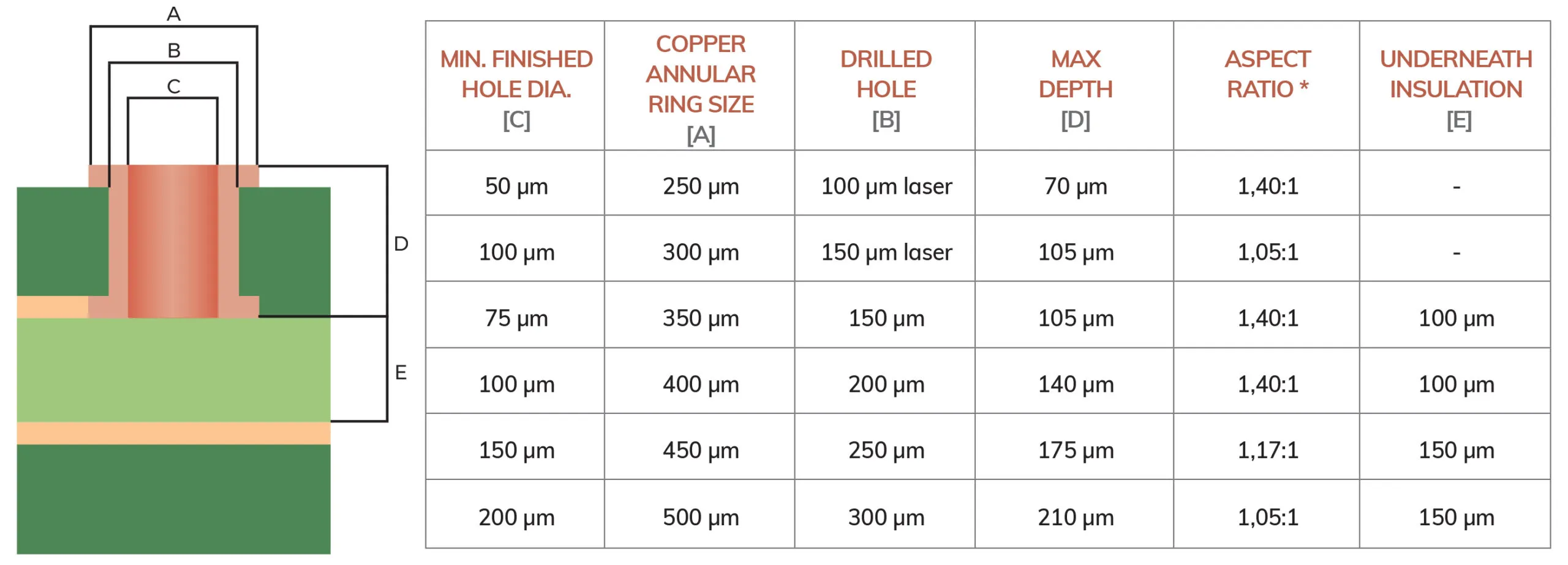
Via Size Guidelines for Optimal Design
Choosing the right via size is critical for both electrical performance and manufacturability. Via size guidelines depend on factors like current-carrying capacity, signal speed, and board thickness. Here are some general recommendations:
- Minimum Via Diameter: For standard designs, a via diameter of 0.3mm to 0.5mm is common. For HDI designs using microvias, diameters as small as 0.1mm may be used, but check with your manufacturer for capabilities.
- Aspect Ratio: The aspect ratio (via depth to diameter) should ideally be below 10:1 to ensure reliable plating during manufacturing. For a 1.6mm thick board, a via diameter of 0.2mm or larger is recommended.
- Current Capacity: Larger vias can carry more current. A 0.5mm via can typically handle 1-2 amps, while a 0.3mm via is better suited for signals with lower current (below 0.5 amps).
Always consult your design software’s design rule checks (DRC) and your manufacturer’s guidelines to ensure via sizes meet both performance and production requirements.
Minimizing Via Inductance for High-Speed Designs
In high-speed PCB designs, vias can introduce parasitic inductance, which affects signal integrity by causing delays or reflections. Minimizing via inductance is essential for maintaining clean signal transmission, especially at frequencies above 500 MHz.
Here are some strategies to reduce via inductance:
- Use Smaller Vias: Smaller diameter vias have lower inductance. For instance, a 0.2mm via has significantly less inductance (around 0.5 nH) compared to a 0.5mm via (around 1.2 nH).
- Shorten Via Length: Use blind or buried vias to reduce the via stub length, which minimizes inductance. A shorter via stub can reduce inductance by up to 50% in some designs.
- Place Return Vias Nearby: Position ground vias close to signal vias to provide a low-inductance return path for high-speed signals. A spacing of 1mm or less is ideal for signals above 1 GHz.
By carefully designing via placement and size, you can keep inductance low and ensure your high-speed signals remain clean and reliable.
Improving Signal Integrity with Vias
Signal integrity is a top concern in modern PCB designs, especially for high-speed and high-frequency applications. Vias play a significant role in maintaining signal quality, and poor via design can lead to issues like crosstalk, reflections, and noise. Here are some tips for improving signal integrity with vias:
- Avoid Via Stubs: Via stubs (unused portions of a via) act as antennas, causing signal reflections. Use back-drilling or opt for blind/buried vias to eliminate stubs in high-speed designs.
- Match Impedance: Ensure the via’s impedance matches the trace impedance. For a 50-ohm trace, design vias with minimal inductance and capacitance to avoid mismatches, which can be simulated using PCB design software.
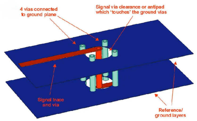
- Use Differential Pair Vias: For differential signals, place vias for the pair close together (e.g., 0.5mm apart) to maintain consistent impedance and reduce crosstalk.
- Ground Shielding: Surround high-speed signal vias with ground vias to shield against interference. A common practice is placing ground vias in a circular pattern around the signal via, spaced at 1-2mm intervals.
By following these practices, you can significantly enhance the signal integrity of your PCB, ensuring reliable performance even at high speeds.
Tools for Designing Vias in PCB Layouts
Modern PCB design software offers powerful tools to help you select and place vias for optimal performance. These tools can simulate signal behavior, check design rules, and even suggest via types based on your board’s requirements. Here are some features to look for:
- Design Rule Checks (DRC): Ensure your software can validate via sizes, spacing, and aspect ratios against manufacturing constraints.
- Signal Integrity Simulation: Use simulation tools to analyze via inductance, impedance mismatches, and signal reflections before finalizing your design.
- Via Wizard Tools: Some software includes wizards or templates for selecting via types (e.g., blind, buried, or microvias) based on layer count and density.
- 3D Visualization: A 3D view of your PCB can help you spot potential issues with via placement and routing across layers.
Leveraging these tools can save time and reduce errors, ensuring your via design aligns with both performance goals and manufacturing capabilities.
Balancing Performance with Manufacturability
While advanced via types like microvias and buried vias offer significant benefits for high-density and high-speed designs, they can also increase manufacturing complexity and cost. It’s important to balance performance needs with practical considerations. For example:
- Cost vs. Complexity: Through-hole vias are cheaper and easier to produce, making them suitable for low-cost or prototype boards. Blind and buried vias, while space-efficient, may increase costs by 20-30%.
- Manufacturer Capabilities: Not all manufacturers can produce microvias or high aspect ratio vias. Always confirm capabilities and minimum tolerances before finalizing your design.
- Testing and Reliability: Advanced vias like microvias may be more prone to defects if not manufactured correctly. Consider adding extra testing steps for critical designs.
By aligning your via choices with both performance goals and production realities, you can avoid costly redesigns and delays.
Conclusion: Making Informed Via Choices for Your PCB
Selecting the right vias for your PCB design is a critical step in achieving optimal performance, reliability, and manufacturability. By understanding via types in PCB design—through-hole vias, blind vias, buried vias, and microvias—you can make informed decisions that suit your project’s needs. Techniques like via stitching, adhering to via size guidelines, minimizing via inductance, and improving signal integrity with vias further enhance your design’s success.
Whether you’re designing a simple two-layer board or a complex multilayer HDI PCB, the principles covered in this guide can help you navigate via selection with confidence. Use the right tools, follow best practices, and collaborate with your manufacturing partner to ensure your vias contribute to a high-performing, cost-effective design.
With careful planning and attention to detail, your PCB design will not only meet technical requirements but also stand out in terms of efficiency and reliability. Keep these tips in mind for your next project, and you’ll be well on your way to creating exceptional electronic products.


